Lithography is the family of processes used to define patterns on a surface so that material can be added, removed or modified in selected locations. It is essential to semiconductor manufacturing, but its reach is much wider: printed circuit boards, advanced packaging, flat-panel displays, microelectromechanical systems, photonics, sensors, microfluidics and optical components all depend on some form of lithography.
There is no single modern lithography technology. Leading-edge logic uses extreme-ultraviolet exposure for selected critical layers while continuing to use deep-ultraviolet scanners for many others. Mature chips may rely on i-line, krypton-fluoride or argon-fluoride tools whose productivity and cost have been refined for decades. Advanced packaging uses steppers, projection aligners and laser direct imaging over thicker resists and less-flat substrates. Electron beams write photomasks and specialized devices; nanoimprint replicates fine three-dimensional structures; directed self-assembly can multiply or regularize patterns created by another technique.
The state of the art therefore lies in selecting and integrating technologies—not replacing every established tool with the shortest wavelength.
The basic patterning cycle
A conventional photolithography sequence begins with a clean substrate. A photosensitive material called resist is applied, usually by spin coating, and baked to remove solvent and establish a controlled film. An exposure system projects or brings a pattern into contact with the resist. Development dissolves selected areas, producing a temporary relief image.
That resist image is rarely the final device. It becomes a mask for etching, ion implantation, deposition, electroplating or another material process. The resist is then stripped, the result is cleaned and measured, and the cycle begins again for another layer. A modern integrated circuit may require more than 100 aligned patterning levels, with different lithography platforms selected according to feature size, overlay tolerance, resist thickness and cost.
Good lithography is an integrated result. Scanner resolution matters, but so do the mask, resist chemistry, wafer topography, focus, dose, post-exposure bake, developer, etch process, contamination control, overlay measurement and statistical process control.
The current lithography toolbox
| Technology | Typical role | Principal strength | Principal challenge |
|---|---|---|---|
| Contact and proximity exposure | MEMS, research, microfluidics and low-cost patterning | Simple equipment and large exposure fields | Mask wear, particles, distortion and limited fine-feature control |
| i-line projection | Power devices, sensors, MEMS, packaging and mature semiconductors | Stable processes, thick-resist capability and attractive cost | Resolution is limited compared with shorter wavelengths |
| KrF DUV | Mature and intermediate semiconductor layers | High productivity and a large installed process base | Fine features require resolution enhancement or another platform |
| ArF dry and immersion DUV | Advanced semiconductor layers and multiple patterning | Excellent overlay, throughput and manufacturing maturity | Multi-patterning increases masks, process steps and edge-placement error |
| 0.33-NA EUV | Critical logic and memory layers | 13.5-nm wavelength reduces some multi-patterning | Tool cost, source power, masks, resist stochastic effects and inspection |
| 0.55-NA High-NA EUV | Future critical layers for sub-2-nm-class logic and advanced memory | Higher resolution and potential return to single exposure for selected pitches | Shallow depth of focus, anamorphic imaging, field stitching, resist and mask readiness |
| Electron-beam lithography | Photomasks, research, quantum devices and low-volume nanostructures | Very high resolution without an optical mask | Serial writing is slow and proximity effects require correction |
| Laser or optical direct write | PCBs, packaging, displays, masks and rapid prototyping | Maskless flexibility and fast design changes | Resolution and throughput depend strongly on field size and application |
| Nanoimprint lithography | Photonics, optics, displays, biotechnology and emerging semiconductor uses | High-resolution replication of two- and three-dimensional relief | Template defects, particles, overlay, residual layer and release |
| Directed self-assembly | Pitch multiplication and pattern rectification | Molecular-scale regularity with relatively simple guiding patterns | Defectivity, placement, design restrictions and integration complexity |
Mature optical lithography remains indispensable
Mercury-lamp g-line and i-line exposure systems continue to manufacture devices whose value comes from voltage handling, sensing, mechanical structures, analog performance or low cost rather than minimum transistor dimension. I-line uses 365-nm light and supports robust thick-resist processes, lift-off, bumping, MEMS and compound-semiconductor fabrication. Projection aligners keep the mask separated from the wafer, while contact aligners trade some mask life and defect control for simple full-field exposure.
These tools are not obsolete. Automotive controllers, power-management chips, image sensors, radio-frequency devices, microfluidics and industrial electronics often use mature nodes. Their factories prioritize yield, equipment availability, process stability and depreciation over the smallest printable line.
Deep-ultraviolet lithography: the high-volume workhorse
Deep-ultraviolet lithography includes krypton-fluoride lasers at 248 nm and argon-fluoride lasers at 193 nm. KrF remains common for mature and less-critical layers. ArF dry scanners extend resolution further, while ArF immersion places a thin water layer between the final projection lens and wafer. The water raises the optical system's numerical aperture beyond what is possible in air; the most advanced immersion systems reach an NA of 1.35.
ASML's explanation of lenses, mirrors and numerical aperture illustrates why wavelength is only one resolution lever. Feature size also depends on numerical aperture and a process factor improved through illumination, masks, resist and computation.
ArF immersion was extended far beyond its original single-exposure limit by multiple patterning. In litho-etch-litho-etch, a dense design is divided between separate masks and exposures. Self-aligned double and quadruple patterning use deposited spacers to multiply pitch with better regularity. These methods enabled advanced logic and memory before EUV reached production and remain important where their mature overlay and process control justify the extra steps.
Multiple patterning carries costs. Every added deposition, etch, clean and exposure increases cycle time, process interaction and opportunity for defect. The critical metric becomes edge placement: the final position of each line depends on overlay, critical-dimension variation, spacer thickness, etch bias and mask error together.
Standard EUV in high-volume manufacturing
Extreme-ultraviolet lithography uses 13.5-nm light, more than fourteen times shorter in wavelength than ArF DUV. Because EUV is absorbed by air and by ordinary optical materials, the light path operates in vacuum and uses multilayer reflective mirrors rather than transmissive lenses. The source forms plasma by striking microscopic molten-tin droplets with powerful laser pulses. A reflective mask carries the pattern.
Production EUV systems use a numerical aperture of 0.33. They print selected critical layers in advanced logic and memory with fewer masks than an equivalent DUV multiple-patterning flow. Other layers on the same chip still use DUV because their dimensions do not justify EUV's cost or complexity. A modern leading-edge fab is therefore a mixed fleet.
EUV's short wavelength does not make patterning automatic. Source power and collector efficiency affect throughput. The reflective mask is a complex multilayer structure whose absorber and topography influence imaging. A thin pellicle protects the mask from particles but must transmit EUV while surviving heat. Actinic inspection—using EUV wavelength—is needed to reveal some defects that other inspection methods may not represent correctly.
The stochastic problem
EUV photons carry high energy, but relatively few photons expose each very small feature. Their arrival and the chemical reactions that follow are statistical. Random local variation can cause missing contacts, merged holes, broken lines or microbridges even when the average feature dimension is correct. Resist molecules, secondary electrons and material granularity add further variation.
Engineers must balance resolution, line-edge roughness and exposure dose. More dose generally improves statistical fidelity but reduces scanner throughput. Chemically amplified resists offer sensitivity through catalytic reactions; metal-oxide resists can improve resolution and pattern-transfer performance in very thin films. Underlayers, post-exposure bake atmosphere and development conditions are now part of the effort to lower dose without sacrificing yield.
High-NA EUV enters the manufacturing ecosystem
High-numerical-aperture EUV raises NA from 0.33 to 0.55 while retaining 13.5-nm light. The stronger focusing improves resolution and image contrast, with the goal of printing features in one exposure that would otherwise require multiple EUV or DUV patterning steps. ASML's EXE platform uses much larger mirrors and anamorphic optics: the mask image is reduced four times in one direction and eight times in the other so established reticle dimensions can remain in use.
High-NA is no longer merely a paper roadmap. ASML shipped its first EXE:5200B in 2025, and imec installed an EXE:5200 in its Leuven pilot line in March 2026. Imec and ASML have demonstrated single-exposure patterns and are developing the complete process around them. In 2025, imec reported more than 90 percent electrical yield for 20-nm-pitch metal test structures patterned in one High-NA exposure using a metal-oxide resist.
The High-NA development program still faces depth-of-focus, stochastic defect, field-stitching, mask, metrology and pattern-transfer challenges. The smaller exposure field created by anamorphic imaging may require stitching for some large designs. Thinner resist helps preserve image fidelity but provides less material to protect the wafer during etch. High-NA will initially be used selectively where its patterning advantage outweighs those integration costs.
Computational lithography is part of every advanced exposure
The mask pattern used in advanced manufacturing often looks unlike the intended wafer geometry. Optical proximity correction adds serifs, biases line widths and reshapes corners so that diffraction and process effects produce the desired result. Source-mask optimization jointly designs illumination and reticle features. Sub-resolution assist features improve the image without intentionally printing.
Inverse lithography starts from the desired wafer result and computationally solves for an often-curvilinear mask. Machine learning can accelerate model calibration, mask optimization, defect classification and process-window prediction. Curvilinear masks are becoming more practical as multibeam electron writers and contour-based inspection improve.
Computational lithography must include more than scanner optics. Modern models account for mask three-dimensional effects, resist behavior, etch bias, wafer topography and stochastic risk. Design-technology co-optimization adjusts standard cells and routing so they can be patterned with adequate margin, instead of asking lithography to rescue an unconstrained design at the end.
Photomasks and reticles
Optical masks use patterned absorbers on transparent substrates. EUV masks are reflective multilayer mirrors with an absorber pattern. Both require extraordinarily low defect levels because a repeating defect can print on every die exposed with that reticle.
Electron-beam mask writers translate design data into the physical reticle. Multibeam writers expose many locations in parallel and are important for complex EUV and curvilinear mask shapes. Mask data preparation fractures designs into writable elements, applies process corrections and manages enormous file sizes. Inspection, review and repair then determine whether the mask is fit for production.
Pellicles, cleaning and handling are as important as writing. A particle on the protected side of an optical pellicle is kept out of focus; EUV pellicles must perform the same protective role in vacuum while absorbing as little 13.5-nm light as possible.
Electron-beam lithography and other charged-particle methods
Electron-beam lithography focuses electrons directly onto an electron-sensitive resist. Because no optical mask is required, it offers high resolution and arbitrary pattern generation. It is standard for writing photomasks and invaluable in research, quantum devices, nanophotonics and low-volume prototypes.
Its limitation is throughput. A focused beam writes serially, and denser areas take longer. Electrons also scatter within the resist and substrate, exposing nearby regions; proximity-effect correction changes local dose to compensate. Charging on insulating substrates, resist contrast, stage accuracy and data volume require careful control.
Multibeam systems improve speed by writing with many beams simultaneously. Electron projection and ion-beam techniques offer additional capabilities for specialized fabrication or repair, but they do not replace optical wafer scanners for mainstream high-volume semiconductor layers.
Laser direct imaging and maskless optical lithography
Laser direct imaging exposes resist from digital data without manufacturing a separate mask. It is widely used for printed circuit boards, where each panel may contain distortion that software can measure and compensate. It is also useful for advanced packaging, display repair, mask fabrication, microfluidics and rapid process development.
Maskless projection systems use spatial light modulators or digital micromirror devices to expose many pixels at once. Direct laser writers can raster or vector-scan a focused spot. Two-photon polymerization confines a nonlinear exposure within a transparent resist, enabling intricate three-dimensional microstructures for research, photonics and biomedical applications.
These methods trade mask cost and turnaround time for writing speed and resolution. They are strongest where designs change frequently, substrates vary or volume does not justify a reticle.
Nanoimprint lithography: high-resolution replication
Nanoimprint forms a pattern by pressing a physical template into a material or liquid resist rather than projecting an optical image. Thermal imprint softens a polymer with heat and pressure. UV nanoimprint fills a transparent template with low-viscosity material and cures it with ultraviolet light. Step-and-repeat systems pattern portions of a wafer, while full-field and roll-to-roll processes address larger surfaces.
The technology can reproduce fine features and true three-dimensional relief with relatively simple optics. It is commercially important in diffractive and meta-optics, augmented-reality waveguides, wire-grid polarizers, light-management films, photonics, biotechnology and microfluidics. EV Group offers full-field and step-and-repeat UV nanoimprint platforms, while Canon is pursuing semiconductor nanoimprint capable of patterns at 15 nm and below.
The physical contact creates distinct challenges. A particle can damage the template or produce repeated defects. Resist must fill every cavity without trapped gas, then release cleanly after cure. Residual-layer thickness must be uniform before pattern transfer. Semiconductor use also demands extremely tight overlay from one imprinted level to the next.
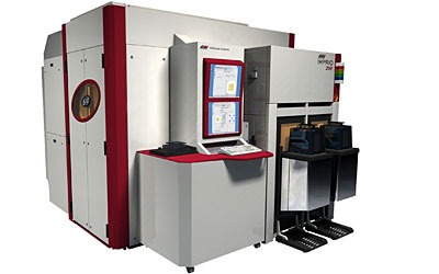
The Imprio 250 described in the original version of this article was an early step-and-flash imprint system from Molecular Imprints. Canon acquired Molecular Imprints' semiconductor business in 2014 and continued development toward current nanoimprint platforms. The core idea survived, but the most established markets today include optical and photonic replication as well as continued evaluation for memory and semiconductor patterning.
Directed self-assembly and pattern multiplication
Block copolymers contain chemically distinct polymer blocks that separate into ordered nanoscale domains. In directed self-assembly, a lithographically produced chemical or topographic guide controls how those domains align. The resulting lines or holes can multiply pitch, improve uniformity or create dense periodic features beyond the guide pattern's native resolution.
DSA is not a completely maskless replacement. Conventional lithography defines the guiding pattern, while the material performs part of the fine pattern formation. Integration requires control of defects, orientation, placement, line-edge roughness and removal of one polymer block. The strongest opportunities are regular patterns in memory, vias and specialized nanostructures where design constraints are acceptable.
Advanced packaging changes the lithography problem
Chiplets and heterogeneous integration have made packaging lithography increasingly important. Redistribution layers, microbumps, copper pillars, interposers, fan-out structures and panel-level packaging require fine lines and accurate overlay across substrates that may be warped, thick or dimensionally unstable.
Packaging tools often prioritize large exposure fields, deep focus, thick-resist processing and local alignment over transistor-scale resolution. Steppers, projection aligners and laser direct imaging compensate for die placement and substrate distortion. Photoresists may be tens or hundreds of micrometers thick for electroplating molds, making sidewall profile and dose uniformity critical.
Hybrid bonding pushes overlay and surface preparation to much tighter levels as copper and dielectric surfaces join with very small pitch. Lithography, deposition, planarization, cleaning, inspection and bonding must be developed as one process flow.
MEMS, compound semiconductors and photonics
MEMS devices often need thick resists, deep etching, double-sided alignment and patterning over topography. Power and radio-frequency semiconductors made from silicon carbide or gallium nitride may use mature optical wavelengths but demand careful control of wafer bow, transparent or semi-insulating substrates and high-temperature process integration.
Photonics combines optical waveguides, gratings, couplers and sometimes three-dimensional surface relief. DUV projection provides high-volume precision for silicon photonics, electron-beam writing supports prototyping and mask creation, and nanoimprint excels at replicating optical textures over large areas.
Resists, underlayers and pattern transfer
Positive resist becomes more soluble where exposed; negative resist becomes less soluble. Chemically amplified systems use exposure to generate a catalyst that drives reactions during post-exposure bake, increasing sensitivity. Molecular and metal-oxide formulations target smaller feature sizes and stronger etch resistance. Dry-film resists serve circuit boards and packaging, while thick epoxy resists create high-aspect-ratio MEMS structures.
As features shrink, resist thickness must often decrease to avoid collapse and preserve imaging. A thin resist may not survive the final etch, so multilayer stacks transfer its image into a silicon-containing layer or hard mask before etching the device material. Patterning performance is therefore judged after transfer, not only by a beautiful top-down resist image.
In 2026, imec reported that controlling oxygen during the post-exposure bake of metal-oxide EUV resist improved dose response, illustrating how process atmosphere can affect throughput and defectivity at the leading edge.
Metrology, inspection and process control
Lithography cannot be controlled by measuring only a few linewidths. Manufacturers monitor critical dimension, overlay, focus, dose, line-edge roughness, film thickness, wafer shape and defectivity. Optical scatterometry provides rapid profile measurements; critical-dimension scanning electron microscopy resolves small features; atomic-force microscopy measures topography; electron-beam inspection finds subtle defects at lower throughput.
Overlay correction now accounts for translation, rotation, magnification, wafer distortion and local process signatures. Advanced process control feeds measurements forward and backward between lots, adjusting scanner and process settings. Virtual metrology predicts results from equipment data, but periodic physical measurement remains necessary to prevent model drift.
At High-NA dimensions, electrical test structures are essential because not every stochastic break or bridge is captured efficiently by image sampling. Imec's 20-nm-pitch High-NA demonstration combined patterned and metallized structures with electrical yield measurements to expose rare failures.
How manufacturers select a lithography method
| Question | Why it matters |
|---|---|
| What is the minimum pitch and shape? | Dense lines, isolated contacts and three-dimensional relief favor different techniques. |
| How much overlay error is tolerable? | A photonic surface may need little layer-to-layer alignment; logic interconnects require nanometer-scale control. |
| What is the substrate? | Silicon wafers, glass panels, flexible films, compound semiconductors and packages differ in flatness and handling. |
| How thick must the resist be? | Fine transistor imaging and deep electroplating molds occupy opposite process regimes. |
| What is the production volume? | A costly reticle and fast exposure suit volume; direct write suits prototypes and frequent revisions. |
| Is the pattern regular or arbitrary? | Self-assembly and imprint are strongest for repeatable structures; direct write offers design freedom. |
| What defect level is acceptable? | A cosmetic optical film and a critical transistor contact carry very different yield consequences. |
| What happens after resist development? | Etch selectivity, deposition and cleaning may determine the required resist stack and profile. |
The current practice is heterogeneous
Lithography's future is not a contest in which one technology eliminates all others. High-volume semiconductor factories will continue mixing i-line, KrF, ArF dry, ArF immersion and EUV according to layer economics. High-NA EUV will be inserted selectively as its process ecosystem matures. Electron beams will write the masks that optical systems project. Nanoimprint will replicate structures that are expensive to form optically. Direct imaging will serve variable products and distorted substrates. Self-assembly will augment guided patterns where molecular regularity adds value.
The common trend is co-optimization. Mask, illumination, resist, scanner, etch, metrology and device design are developed together. At the smallest dimensions, the exposure tool alone no longer defines what can be manufactured. The winning practice is the complete patterning system that achieves acceptable resolution, overlay, defects, throughput and cost on the finished device.