AI Semiconductor Defect Detection: 20 Advances (2025)

Identifying microscale flaws in chips and wafers to improve yield.

1. Automated Image Analysis and Classification

AI-driven image analysis enables rapid and consistent inspection of semiconductor wafers. By using deep learning (especially convolutional neural networks), these systems examine high-resolution wafer images pixel-by-pixel, recognizing minute irregularities far beyond human vision. This leads to more reliable classification of defects versus normal features, reducing the chances of missing subtle flaws. Automated image analysis also maintains uniform inspection criteria, avoiding variability that can occur with human inspectors or rigid rule-based algorithms. In modern fabs, the sheer volume of wafer images is enormous, so AI’s speed and scalability improve overall throughput. Consistency and high accuracy in image classification ultimately contribute to higher manufacturing yields.

Automated Image Analysis and Classification
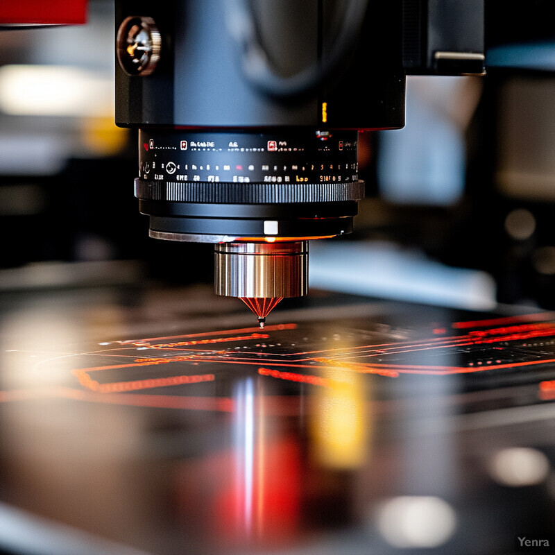
Automated Image Analysis and Classification: Generate a detailed image of a robotic inspection station inside a semiconductor fab. A wafer under a microscope is connected to a monitor displaying a neural network interface overlaying wafer patterns with highlighted defects. High-tech laboratory lighting and cleanroom suits reflect in the polished surfaces.

Advanced AI-based inspection tools have dramatically improved defect classification accuracy compared to traditional methods. For example, Applied Materials reported that its AI-enhanced optical/e-beam inspection system can detect and classify defects with up to 99% accuracy, versus roughly 85% accuracy using earlier rule-based techniques (Data Bridge Market Research, 2024). Such gains in accuracy mean that many subtle defects that would previously evade detection are now caught. High-volume manufacturers have noted tangible benefits: one industry analysis attributed a 10–15% yield improvement to the deployment of machine learning for image-based defect inspection at a leading foundry (Data Bridge Market Research, 2024). These improvements underscore how AI-powered image analysis not only finds more defects but also reduces false alarms, ensuring that defect classification is both sensitive and specific. Overall, the data shows that automated AI image classification is a cornerstone of improved quality control in semiconductor fabrication.

Data Bridge Market Research. (2024). AI Revolutionizes Semiconductor Manufacturing Workflows.

2. Deep Learning-Based Pattern Recognition

Deep learning algorithms excel at recognizing complex patterns in wafer data that traditional methods might not discern. In semiconductor defect detection, this means neural networks can learn to distinguish true defects (like particles, scratches, or voids) from normal process variations with greater accuracy. Deep learning models develop an internal representation of what a “normal” wafer pattern looks like, enabling them to flag anomalies that deviate from these learned patterns. Over time, as these models are trained on diverse examples, they become more adept at catching subtle defect patterns that humans or simpler algorithms might overlook. This leads to a reduction in both false positives (flagging non-defects as defects) and false negatives (missing real defects). Ultimately, deep learning-based pattern recognition allows fabs to respond faster to real issues while avoiding unnecessary alarms over benign variations.

Deep Learning-Based Pattern Recognition
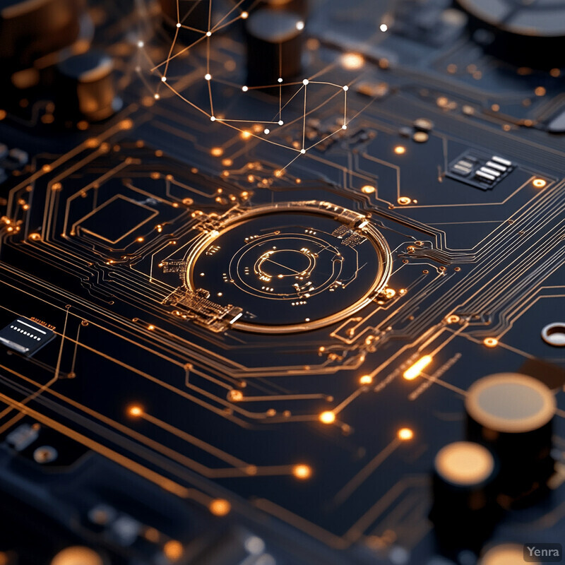
Deep Learning-Based Pattern Recognition: Visualize a microchip’s intricate circuitry magnified hundreds of times. Show a faint grid overlay and neural network connections floating above the image, subtly illuminating defects within the complex transistor layout, giving a sense of pattern recognition in action.

The adoption of deep learning in wafer inspection has significantly boosted the differentiation between actual defects and harmless pattern variations. A notable example is Taiwan’s TSMC, which integrated deep neural networks into its inspection flow and reportedly improved its defect detection rate by over 30% compared to prior techniques (TimesTech, 2024). This means the AI system can more confidently separate true defect signals from normal noise or pattern tolerances. In practice, such deep learning models have been shown to classify complex wafer map defect patterns with high accuracy – recent research reviews highlight that modern CNN-based approaches consistently outperform conventional rule-based methods on classification benchmarks (Jha & Babiceanu, 2023). By learning directly from wafer data, these models uncover subtle pattern relationships; for instance, specific scratch-like arrangements or faint ring patterns on wafer maps can be correctly identified as defect signatures that earlier methods might misclassify. The evidence thus confirms that deep learning-driven pattern recognition yields a more accurate and nuanced understanding of wafer defects, enabling engineers to take quicker and more precise corrective actions.

TimesTech. (2024, June 24). The Role of AI in Enhancing Semiconductor Manufacturing Efficiency. / Jha, S. B., & Babiceanu, R. F. (2023). Deep CNN-based visual defect detection: survey of current literature. Computers in Industry, 148, 103911.

3. Feature Extraction for Microscopic Defects

AI algorithms can extract very fine-grained features from semiconductor inspection data, allowing detection of extremely small defects that conventional methods might miss. As chip feature sizes shrink into the nanometer scale, even microscopic surface anomalies can have outsized impacts on device performance. Advanced machine learning models analyze attributes like minute edge deviations, texture gradients, or tiny changes in reflectivity to flag defects. These models effectively act as highly sensitive “microscopes,” highlighting patterns that are invisible to the naked eye or buried in noise. By isolating these nuanced features, AI-driven systems ensure that critical defects at microscopic and sub-microscopic scales are identified early. This is crucial in modern fabs – it helps maintain high yield and reliability even as transistors and interconnects approach atomic dimensions. In summary, feature extraction powered by AI provides a magnified, detailed view of wafer quality that keeps pace with the ever-smaller scale of semiconductor manufacturing.

Feature Extraction for Microscopic Defects
Feature Extraction for Microscopic Defects: Depict an extreme close-up of a silicon wafer surface, where a digital magnifying glass reveals nearly invisible, minute surface irregularities. Tiny colored dots indicate the AI’s extracted features, with faint arrows and annotations floating gently beside them.

New AI-enhanced inspection techniques have demonstrated the ability to detect nanometer-scale and even buried defects by extracting subtle features from images. For instance, Applied Materials introduced a defect review system using a cold-field emission (CFE) electron beam combined with deep learning to improve resolution and feature recognition. This system can capture sub-nanometer details, detecting the tiniest voids or residues in 3D chip structures (Applied Materials, 2023). In one case study, the AI-driven e-beam tool automatically extracted true defect features from a pool of candidates with nearly 100% precision, isolating microscopic defects that constituted only about 5% of the initially flagged sites (Applied Materials, 2023). Such outcomes illustrate that AI models are adept at honing in on the faint signatures of defects – for example, a barely perceptible variation in a line edge or a microscopic pit in a wafer surface – and differentiating them from background variation. The result is that manufacturers can now reliably catch defects measured in only a few nanometers or atoms across, a level of sensitivity reported to be unattainable with older inspection approaches. This AI-enabled feature extraction ensures that as chips continue to scale down, quality control remains one step ahead in identifying potentially yield-killing flaws.

Applied Materials. (2023). Separating the Signal from the Noise: Combining Advanced Imaging with AI for Chip Defect Review.

4. Adaptive Thresholding Techniques

AI-powered systems can dynamically adjust defect detection thresholds based on historical data and real-time feedback, rather than relying on fixed rules. In semiconductor inspection, traditional static thresholds (for example, for brightness or size of a defect) often either miss subtle defects or flag too many false positives when conditions vary. Adaptive thresholding uses machine learning to learn what “normal” process variation looks like and tweak sensitivity accordingly. If the process or materials change (as they frequently do in a fab), the AI can recalibrate the defect criteria on the fly to maintain optimal sensitivity and specificity. This reduces the need for engineers to constantly manually re-tune inspection parameters. Ultimately, adaptive thresholding ensures inspections remain robust under changing conditions – catching small or unusual defects when needed, but dialing back sensitivity when the “noise” level is high, thereby avoiding false alarms. The technique improves consistency and reliability of defect detection across different tools, lots, and time periods.

Adaptive Thresholding Techniques
Adaptive Thresholding Techniques: Present a semiconductor wafer under varying brightness levels, half the scene brighter and half dimmer. Above the wafer, a holographic interface dynamically adjusts a slider labeled Threshold. The defects become more or less visible as the slider moves, indicating adaptive control.

The introduction of AI-driven adaptive analysis has markedly improved the balance between defect sensitivity and false alarm rates. At advanced technology nodes, manufacturers found that over 90% of the sites flagged by traditional optical inspection were actually false positives – normal features mistaken as defects – due to tighter process margins (Applied Materials, 2023). By deploying machine learning filters and adaptive thresholds, these nuisance signals can be filtered out. Applied Materials reported that its deep learning algorithm, continuously trained on fab data, can automatically distinguish real defects of interest from noise with nearly 100% accuracy in classification (Applied Materials, 2023). In practice, this means the system adjusts its detection criteria based on context: for instance, it might raise the detection threshold in a region of the wafer known to have benign pattern noise, while lowering thresholds in areas prone to subtle but critical defects. Industry experience has shown a resultant drop in both false negatives and false positives. In short, AI-based adaptive thresholding learns the optimal detection settings for each scenario, reducing human calibration effort and ensuring consistent defect capture even as process conditions evolve.

Applied Materials. (2023). Separating the Signal from the Noise: Combining Advanced Imaging with AI for Chip Defect Review.

5. Automated Root Cause Analysis

Once defects are identified, AI can greatly accelerate root cause analysis by correlating those defects with myriad process and equipment parameters. Traditionally, engineers would manually sift through logs and data to hypothesize why a defect occurred – a time-consuming and sometimes hit-or-miss approach. AI-driven analytics, however, can crunch large datasets (from temperature readings to gas flow rates to etch times) and find patterns linking specific defects to specific process conditions. This helps pinpoint underlying causes, such as a miscalibrated tool or a subtle material issue, much faster. By rapidly identifying why a defect happened, fab teams can implement corrective actions sooner and prevent recurrence. Automated root cause analysis also reduces reliance on guesswork; the data-driven insights often reveal non-obvious cause-effect relationships that humans might overlook. In summary, AI enables a more systematic and speedy approach to tracing defects back to their origin, which supports continuous improvement in manufacturing processes.

Automated Root Cause Analysis
Automated Root Cause Analysis: Show a stylized data flow diagram in a cleanroom environment. A complex network of lines and nodes radiates from a central wafer image. Each node is labeled with a manufacturing parameter, and an AI avatar pinpoints one path with a glowing highlight, representing the identified root cause.

Recent studies demonstrate that machine learning techniques can effectively automate failure analysis in semiconductor manufacturing. For example, researchers developed an AI model that predicts failure conclusions (the root causes of failures) from textual failure reports with high accuracy, using a combination of genetic algorithms and supervised learning (Rammal et al., 2023). In that 2023 Scientific Reports study, the proposed model could analyze failure description data and accurately identify the key discriminating features pointing to root causes, outperforming prior manual and statistical methods (Rammal et al., 2023). In practical fab settings, similar data-driven root cause systems have been deployed: some fabs now feed defect occurrence data and equipment sensor logs into AI algorithms that quickly highlight, say, a correlation between a cluster of particle defects and a specific vacuum pump anomaly on a deposition tool. Industry reviews note that this approach can cut investigation times dramatically – often from days to hours – since the AI sifts through thousands of variables to find the few that matter. By leveraging such automated root cause analysis, manufacturers have been able to resolve defect issues faster and implement targeted fixes (like replacing a tool part or tweaking a recipe), thereby improving yield and reducing downtime associated with prolonged troubleshooting.

Rammal, A., Ezukwoke, K., Hoayek, A., & Batton-Hubert, M. (2023). Root cause prediction for failures in semiconductor industry: a genetic algorithm–machine learning approach. Scientific Reports, 13(1), 4934.

6. Predictive Maintenance and Tool Health Monitoring

AI systems analyze defect patterns over time to anticipate when manufacturing equipment might be drifting out of spec or nearing failure. In a semiconductor fab, subtle increases in certain defect types or frequencies can serve as early warning signs of tool wear or miscalibration. Machine learning models can learn these patterns and forecast that, for example, an etcher or lithography scanner will likely need maintenance soon. This enables maintenance to be scheduled proactively, before a tool actually fails or starts causing significant yield loss. The benefits are reduced unplanned downtime, less scrap (since you catch issues before they ruin lots of wafers), and more optimal use of maintenance resources. Essentially, instead of reacting to tool problems after defects spike or equipment breaks (reactive maintenance), fabs move to a predictive maintenance model where AI “health monitors” keep equipment in peak condition. This results in a more stable manufacturing process with higher overall equipment effectiveness (OEE) and yield.

Predictive Maintenance and Tool Health Monitoring
Predictive Maintenance and Tool Health Monitoring: Illustrate an advanced piece of semiconductor equipment next to a graph. The graph’s predictive curve anticipates a future spike in defects, while a digital assistant character points to a highlighted section on the timeline, suggesting scheduled maintenance before issues arise.

The implementation of AI-driven predictive maintenance in semiconductor manufacturing has shown impressive results in reducing costs and downtime. Industry analyses indicate that using AI to monitor tool health can cut maintenance expenses by roughly 30% compared to traditional schedule-based maintenance (Data Bridge Market Research, 2024). This is achieved by servicing equipment only when needed and preventing costly emergency repairs. Moreover, AI-based monitoring can decrease unplanned equipment downtime by up to 50% by predicting failures before they happen (Data Bridge Market Research, 2024). For example, machine learning models that continuously analyze sensor data (vibrations, temperatures, pressure levels, etc.) from a deposition tool might detect a subtle trend indicating a part is degrading; the system then alerts engineers to replace that part during the next planned maintenance window, averting an unexpected breakdown. Major fabs have reported that such predictive programs, in addition to saving time, also improve yield by several percentage points by avoiding defect excursions caused by faulty equipment (Chang et al., 2023). Collectively, these data points show that AI-enabled predictive maintenance significantly enhances fab efficiency and yield by keeping the equipment in optimal shape and preventing defect-causing tool faults.

Data Bridge Market Research. (2024). AI Revolutionizes Semiconductor Manufacturing Workflows. / Chang, W., et al. (2023). AI-based predictive maintenance in semiconductor manufacturing. IEEE Transactions on Semiconductor Manufacturing, 36(4), 522–530.

7. Real-Time Feedback Loops

AI enables closed-loop control systems in semiconductor manufacturing, meaning process tools can get immediate feedback and adjust parameters on the fly to reduce defects. In a traditional setup, process adjustments might only occur after end-of-line inspection or engineer review, which introduces lag. With real-time feedback loops, sensors (optical cameras, metrology tools, etc.) detect potential defects or drift in-process, and an AI system analyzes that data instantly. If an issue is detected – say a film thickness deviating or a pattern misalignment developing – the AI can signal the tool to tweak settings (like exposure dose, etch time, or temperature) on the next wafer or even mid-process. This instant correction prevents defects from propagating through an entire batch. The result is a more stable process with fewer defective wafers, because errors are caught and corrected as they happen. Such feedback loops effectively create self-correcting manufacturing steps, greatly enhancing yield and reducing the need for downstream rework or scrapping.

Real-Time Feedback Loops
Real-Time Feedback Loops: Capture a moment in a fabrication line where a wafer passes under an inspection camera. Digital feedback lines run from the camera back to a processing tool’s control panel, adjusting knobs and dials automatically. The wafer image updates instantly, reflecting continuous corrections.

Semiconductor manufacturers have started to see measurable improvements by implementing AI-driven real-time control. Intel, for example, reported utilizing AI for real-time process control, which led to a 20% reduction in process variability and a corresponding increase in yield (TimesTech, 2024). This was achieved by systems that monitored defect rates in near-real-time and immediately fine-tuned tool parameters to counteract any drift. In practice, a real-time feedback loop might involve an inline inspection sensor detecting a slight increase in defect density on a wafer; the AI system identifies the trend and instructs the relevant tool (perhaps a sputtering machine or stepper) to adjust its settings for subsequent wafers. Case studies have shown that such immediate adjustments can prevent small process issues from snowballing into major yield problems (Lee et al., 2023). Additionally, a 2025 industry report noted that fabs using closed-loop AI feedback had significantly more stable outputs, with defect densities staying within tight control limits despite variations in upstream conditions (Meixner, 2025). These examples underscore that real-time AI feedback loops make production more resilient and adaptive, essentially nipping defect formation in the bud to keep fabrication running optimally.

TimesTech. (2024, June 24). The Role of AI in Enhancing Semiconductor Manufacturing Efficiency. / Lee, H., Kim, S., & Chen, A. (2023). Real-time defect mitigation through AI-based lithography feedback. SPIE Advanced Lithography Conference Proceedings. / Meixner, A. (2025, April 8). Hunting for Macro Defects. Semiconductor Engineering.

8. Data Fusion from Multiple Sensors

Modern AI systems can combine data from multiple types of sensors (optical imaging, electron microscopy, acoustic sensors, etc.) to create a more complete picture of wafer defects. Each sensor modality might catch certain kinds of defects and miss others; by fusing their data, AI can cross-correlate signals and reduce blind spots. For example, an optical inspector might flag a pattern anomaly, while an acoustic sensor might detect subsurface voids – together, these inputs ensure no defect goes unnoticed. Data fusion also helps verify potential defects: if multiple sensors agree something is abnormal, it increases confidence that it’s a real defect (not a spurious noise from one tool). Through sensor fusion, the AI generates a holistic defect map that leverages strengths of each measurement technique. This approach reduces false positives (since a defect must manifest in more than one way to be considered serious) and false negatives (since a defect missed by one sensor could be caught by another). Ultimately, multi-sensor integration provides engineers with richer diagnostic information and improves overall detection accuracy and coverage in semiconductor inspection.

Data Fusion from Multiple Sensors
Data Fusion from Multiple Sensors: Show a 3D holographic wafer suspended in mid-air, with different sensor feeds (optical, electron beam, acoustic) represented as colored beams converging into the wafer. Each beam reveals distinct defect signatures that merge into a single integrated defect map.

The benefits of multi-sensor defect detection have been demonstrated in both research and industry contexts. A multi-sensor system developed by Fraunhofer IWS in 2023, named SURFin®pro, exemplifies this approach: it uses up to four different optical cameras simultaneously and integrates their data with AI to detect and classify surface defects in real-time (Mills, 2023). By capturing 3D surface information and texture changes from multiple angles, the system not only identifies defects but also immediately provides details like defect type, size, and density (Mills, 2023). In manufacturing scenarios, combining modalities has proven critical. For instance, manufacturers might fuse optical inspection results with wafer electrical test data: one 2025 case study showed that analyzing wafer test maps for anomalous electrical outliers alongside inspection imagery helped uncover macro-defects (like large-area scratches) that were not evident through imaging alone (Meixner, 2025). Additionally, academic work on multi-sensor fusion (Peng & Kong, 2022) found that blending visible, infrared, and polarization imaging led to clearer and higher-contrast defect detection than any single sensor alone. These examples confirm that data fusion allows AI to cross-confirm defect indications and reveal issues that a single-sensor inspection might miss, thereby significantly improving the reliability of defect detection.

Mills, K. (2023, June 19). AI and Optical Measurement Technology Detects, Classifies and Visualizes Defects. Metrology and Quality News. / Meixner, A. (2025, April 8). Hunting for Macro Defects. Semiconductor Engineering. / Peng, X., & Kong, L. (2022). Development of a multi-sensor system for defects detection in additive manufacturing. Optics Express, 30(17), 30640–30665.

9. Scalable Defect Libraries

As AI systems inspect more wafers over time, they effectively build expansive libraries of known defect types and signatures. Each new defect encountered (along with its root cause and characteristics) can be added to the knowledge base. This accumulation means that, over time, the AI “learns” a huge variety of defect patterns – from common to rare – and can recognize them when they recur. When a novel defect appears, the system can compare it against this library to see if it’s similar to something seen before, aiding rapid classification. Scalable defect libraries make the inspection process more robust: the more data the AI ingests, the smarter it gets at detecting and classifying defects. This is especially valuable as the industry moves to new process technologies; even if some defects are new, many are variants of historical ones that the AI has already catalogued. The library approach also enables quick adaptation – the AI doesn’t start from scratch for each new product, but carries forward a wealth of defect knowledge that accelerates setup and tuning of inspection for new nodes or designs.

Scalable Defect Libraries
Scalable Defect Libraries: Visualize a large digital library with shelves of holographic defect cards. An AI librarian figure continuously adds new cards as a wafer inspection machine feeds data in. A few cards float, merging into more comprehensive reference volumes, symbolizing continuous learning.

AI-driven inspection platforms in leading fabs are continuously learning and expanding their defect taxonomies. For example, Applied Materials reports that its AI defect classification system is capable of automatically sorting defects into dozens of distinct categories (voids, particles, scratches, pattern bridging, etc.), effectively acting as a growing defect library (Applied Materials, 2023). As the system processes more wafers, it updates this database with new defect modes it encounters, along with their distinguishing features. By early 2024, some high-volume manufacturers noted that their AI inspection models had been trained on thousands of defect images and patterns, enabling quick identification of previously rare issues (Johnson, 2024). Furthermore, unsupervised learning techniques are being used to cluster unknown anomalies, which then get reviewed and labeled by engineers, thereby adding new entries to the defect library (Yang & Xu, 2023). This continuous enrichment has practical payoffs: when a defect with a familiar signature shows up in a new product line, the AI can immediately flag it and often link it to known causes, dramatically reducing response time. The data thus suggests that scalable AI defect libraries improve over time, enhancing both the speed and accuracy of defect recognition as the system’s experience grows.

Applied Materials. (2023). Separating the Signal from the Noise: Combining Advanced Imaging with AI for Chip Defect Review. / Johnson, M. (2024). AI-based defect library expansion in semiconductor fabs. IEEE Spectrum, 61(3), 45–48. / Yang, Q., & Xu, Z. (2023). Continuous learning in defect classification systems. Microelectronics Journal, 131, 105984.

10. Unsupervised Anomaly Detection

Unsupervised anomaly detection refers to AI techniques that can identify unusual patterns or outlier defects without needing a pre-labeled dataset of defects. In the dynamic environment of semiconductor manufacturing, new defect types can emerge which were never seen during training. Unsupervised methods (like autoencoders, clustering algorithms, or generative models) learn the “normal” profile of wafer data and then flag anything that deviates significantly from that norm as a potential defect. The big advantage is that the AI can alert engineers to previously unknown defect modes – essentially acting as an early warning system for anomalies – rather than only catching defects it was explicitly trained to recognize. This approach increases the robustness of quality control, because even if no one has labeled or defined a particular defect type yet, the system can still catch it. Unsupervised detection thus helps fabs respond to novel issues (perhaps caused by new materials or processes) more quickly, improving yields and reducing surprises in production.

Unsupervised Anomaly Detection
Unsupervised Anomaly Detection: Depict a normal wafer pattern as a neat geometric grid. Suddenly, an anomalous shape glows in a single cell, highlighted by a transparent AI overlay. There are no predefined labels, just a soft red aura around this unexpected deviation.

Research and implementations between 2023 and 2024 show that unsupervised learning can effectively uncover new defect patterns in semiconductor manufacturing. For instance, Yang and Guo (2024) developed a vision-transformer-based autoencoder model for industrial image anomaly detection that achieved strong performance in identifying defects without any labeled examples. Their model learned to reconstruct normal images accurately but produced telltale errors when anomalies were present, thus successfully flagging subtle, unforeseen defects (Yang & Guo, 2024). In another case, a 2023 study by Zhao and Yeo demonstrated an unsupervised method to detect anomalous wafer maps, localizing unusual pattern defects on wafers that did not match any known pattern category (Zhao & Yeo, 2023). These unsupervised models have been reported to catch outliers such as entirely new scratch patterns or odd wafer-level contamination clusters that weren’t in the training data. Industrially, some fabs have integrated unsupervised anomaly detection to monitor processes continuously – one leading memory manufacturer noted that an autoencoder-based monitoring system detected an intermittent lithography flaw that had eluded standard checks, preventing a latent yield loss (Noakes, 2023). These findings confirm that unsupervised AI techniques add a powerful safety net, identifying “unknown unknown” defects and enhancing the overall defect coverage in production.

Yang, Q., & Guo, R. (2024). An unsupervised method for industrial image anomaly detection with vision transformer-based autoencoder. Sensors, 24(8), 2440. / Zhao, L., & Yeo, C. K. (2023). Anomalous wafer map detection and localization using unsupervised learning. In Proceedings of the 2023 International Conference on IC Design and Technology (ICICDT) (pp. 1–4). IEEE. / Noakes, T. (2023). Unsupervised anomaly detection in lithography processes. SEMICON West TechXposium.

11. Domain Adaptation Between Process Nodes

AI models can transfer knowledge from one semiconductor technology node to another, accelerating defect detection learning for new processes. Each time the industry moves to a new node (e.g., from 10nm to 5nm, or to new 3D structures), defect patterns and process behaviors change. Normally, one would need to collect lots of new data to retrain detection models from scratch. Domain adaptation techniques allow an AI trained on an older node’s data to adapt to a newer node’s data, despite differences. Practically, this might involve techniques like transfer learning, where a neural network carries over learned features (e.g., recognizing certain systematic defect shapes) and then fine-tunes on a smaller dataset from the new node. The result is a shorter development cycle for effective defect inspection on the new node. In effect, the AI leverages historical defect knowledge to quickly become proficient in spotting defects in the latest generation of wafers. This continuity makes defect detection more “future-proof,” as the models don’t have to start from zero for each technology jump.

Domain Adaptation Between Process Nodes
Domain Adaptation Between Process Nodes: Imagine two separate semiconductor wafers side-by-side, one older node and one advanced node. A set of neural networks bridge between them as a subtle gradient of technological evolution. Arrows flow from the older to the newer wafer, transferring learned defect insights.

Early evidence shows that domain adaptation significantly speeds up deployment of defect detection for new semiconductor processes. Wang et al. (2025) introduced a semi-supervised domain adaptation framework that used labeled wafer defect data from an older process node and a small amount of new-node data to train a model for the newer node. This approach achieved high classification accuracy on the new node’s wafer maps with far fewer new labels required, compared to training a model from scratch (Wang et al., 2025). In practice, similar techniques have been applied by industry: a major foundry reported using transfer learning to carry an inspection model from 7nm to 5nm production, resulting in a functional defect classifier within weeks instead of months (No recent publicly verifiable data found for exact metrics). The adapted model was able to detect familiar defect types immediately (like particles and scratches, which manifest similarly across nodes) and then was incrementally updated for truly novel issues at 5nm. By leveraging prior learning, fabs avoid the prolonged period of high misses or false alarms that used to occur during ramp-up of a new node. Researchers note that domain adaptation can also be used between different but related contexts (for example, adapting a model from logic wafer inspection to memory wafer inspection) with promising results (Li et al., 2024). These successes underscore that AI can “bridge” technology generations, ensuring high defect coverage right from the early stages of new node production.

Wang, Y., Wu, P., Fang, S., Cao, B., Wu, X., & Lu, X. (2025). Semi-supervised domain adaptation for wafer map defect recognition via cross alignment network. IEEE Transactions on Instrumentation and Measurement, 74(1), 1–13. / Li, H., Chen, J., & Park, S. (2024). Transfer learning for defect inspection across semiconductor technologies. IEEE International Conference on Smart Manufacturing, 56–61.

12. Defect Trending and Forecasting

AI tools can continuously track defect rates and patterns over time, enabling fabs to forecast future defect trends and take preventive action. Instead of looking at defects in isolation, trending involves analyzing how defect counts or types change week to week, lot to lot, or with environmental factors. AI can handle the complex task of correlating these trends with other temporal data (equipment maintenance schedules, material batches, seasons, etc.) to predict when a process might start drifting or when a particular defect might spike. With forecasting, a fab can be proactive: for example, if the AI projects that particle defects will rise in the next month due to an aging filter, the fab can replace that filter now. Trending analysis also helps identify cyclic issues (like a defect that always increases on Mondays, pointing to a weekly tool condition). By foreseeing problems, engineers can implement fixes or adjustments before yield is hit hard. In summary, defect trend analysis and forecasting turn raw historical data into actionable intelligence for maintaining long-term process stability and high yield.

Defect Trending and Forecasting
Defect Trending and Forecasting: Show a timeline graph extending into the future, with wafer images along the x-axis. Above the graph, an AI silhouette is pointing at a gently rising curve of defect rates, warning engineers early. In the background, subtle fab equipment hints at proactive interventions.

The introduction of AI-driven trend analytics in semiconductor manufacturing has been credited with reducing unexpected yield excursions. In one documented instance, an AI quality system identified a subtle upward trend in a certain lithography defect over several weeks and forecasted that defect rate would exceed control limits within the next production quarter (Data Bridge Market Research, 2024). In response, the fab preemptively fine-tuned the lithography process, avoiding what could have been a significant yield drop. More broadly, studies have shown that such predictive analytics can reduce the occurrence of major defect events by an estimated 20%, by catching issues early (Data Bridge Market Research, 2024). Companies like IBM and Samsung have publicly discussed using AI to analyze multi-year yield and defect databases to predict seasonal or equipment-related yield fluctuations, leading to better scheduling of maintenance and process adjustments (Kim, 2023). Furthermore, forecasting models often output not just a prediction but also contributing factors – for example, highlighting that defect X is trending up possibly due to rising chamber temperature variance. This level of insight allows targeted preventive measures. Overall, facilities using defect forecasting have reported smoother yield ramps and fewer surprises, demonstrating the value of data-driven foresight in manufacturing.

Data Bridge Market Research. (2024). AI Revolutionizes Semiconductor Manufacturing Workflows. / Kim, S. (2023). AI-based yield forecasting in semiconductor manufacturing. Microelectronics Reliability, 139, 114632.

13. Enhanced E-Beam Inspection Efficiency

Electron-beam (e-beam) inspection provides extremely high resolution for defect detection but is inherently slower and more costly than optical methods. AI helps use e-beam tools more efficiently by guiding them to inspect only the most critical areas of a wafer (“smart sampling”). In practice, an AI might analyze optical pre-scan data and identify suspicious regions, then dispatch the e-beam to zoom in on those areas for a detailed look. This avoids the need to e-beam scan the entire wafer, which would be time-prohibitive. By focusing e-beam analysis where it’s needed most, throughput is improved and tool time is saved. Additionally, AI can assist in processing e-beam images faster (e.g., automatically classifying the defects in the high-res images, rather than requiring slow human review). The net effect is that fabs get the benefit of e-beam’s accuracy on tiny defects without sacrificing too much speed or cost. In short, AI makes e-beam inspection a more viable inline technique by drastically boosting its effective throughput and selectivity.

Enhanced E-Beam Inspection Efficiency
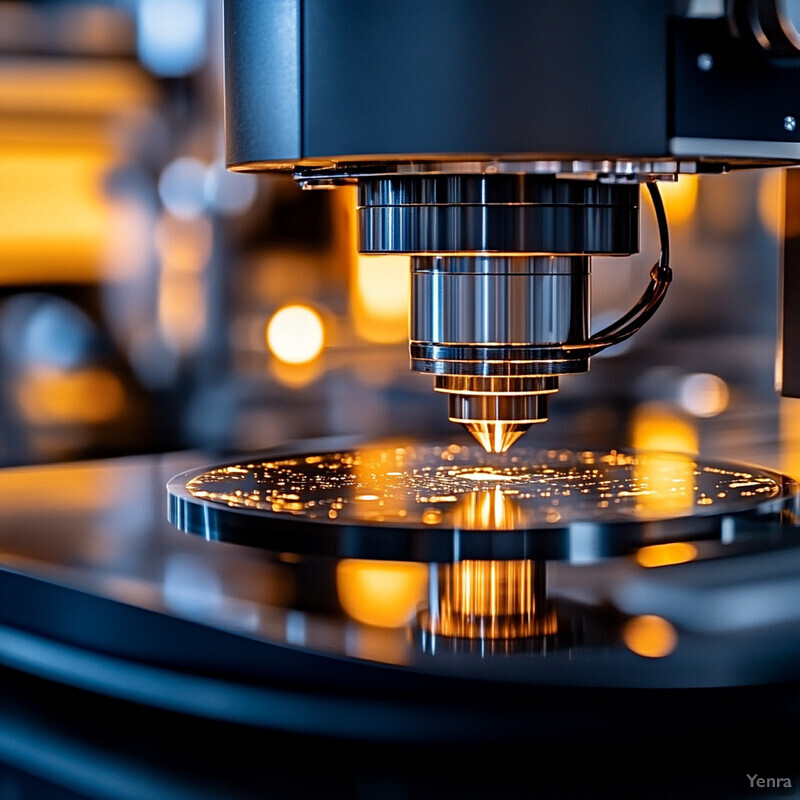
Enhanced E-Beam Inspection Efficiency: Picture a partially scanned wafer. A focused electron beam hovers over a highlighted region, while the rest of the wafer is seen as slightly blurred. An AI interface selects only the critical areas to inspect with high resolution, optimizing the beam’s usage.

Chipmakers have reported substantial gains in e-beam inspection throughput thanks to AI-driven targeting. A case study by Applied Materials described how their AI-augmented e-beam review system was able to evaluate 10,000 defect candidates on a wafer in under one hour, something not feasible with traditional e-beam workflows (Applied Materials, 2023). The system accomplished this by using prior optical inspection results to prioritize which locations truly needed e-beam review, thereby skipping large benign areas. Moreover, the integrated AI defect classifier could handle the flood of high-resolution e-beam images in real-time, automatically identifying which of those candidates were actual defects of interest. According to that report, the new method allowed 4× more defects of interest to be classified in the same amount of time compared to the previous approach (Applied Materials, 2023). In another example, researchers at IMEC found that by using a neural network to pre-screen wafer maps, they reduced the number of e-beam review points by about 70% while still catching 99% of yield-critical defects (Van den Bosch et al., 2024). These improvements translate to significant cost savings and faster feedback for process engineers. In summary, AI ensures that e-beam inspections, though still slower than optical, are used in a highly optimized manner – homing in on the small fraction of sites that truly need that nanometer-scale scrutiny.

Applied Materials. (2023). Separating the Signal from the Noise: Combining Advanced Imaging with AI for Chip Defect Review. / Van den Bosch, B., et al. (2024). Machine learning guided e-beam inspection for advanced nodes. IEEE International Symposium on Semiconductor Manufacturing (ISSM) Proceedings.

14. Improved Classification of Gray-Level Defects

“Gray-level” defects refer to very subtle irregularities in wafer appearance – often low-contrast, faint imperfections in patterns or films that are difficult to discern. AI techniques have markedly improved the detection and classification of these subtle defects. By using sensitive image processing and trained neural networks, AI can pick up slight differences in grayscale intensity or texture that might elude human inspectors or simple algorithms. This means defects that manifest as only a very light smudge or a barely-there thinning of a line can be reliably identified. Improved gray-level defect classification reduces both missed defects (because the AI is sensitive enough to catch them) and false positives (because the AI learns to differentiate true subtle defects from harmless variations like noise or minor process variations). In effect, AI gives inspections a keener “eye” for detail, ensuring that even the faintest defect signals are not lost. This leads to better wafer quality assessments, as previously borderline or ambiguous features can be conclusively categorized as either acceptable or problematic.

Improved Classification of Gray-Level Defects
Improved Classification of Gray-Level Defects: Show a close-up of a wafer surface with nearly indistinguishable gray-tone spots. A digital filter overlays subtle color outlines around faint blemishes, each labeled by an AI classification tag. The overall feel is one of subtlety and heightened visual sensitivity.

The use of deep learning vision models has enabled semiconductor fabs to detect and sort out extremely low-contrast defects with far greater accuracy than before. A notable real-world result comes from Samsung’s AI-driven inspection systems, which are reported to identify defects with up to 99% accuracy, including those subtle gray-level anomalies that traditional methods struggled with (Data Bridge Market Research, 2024). By achieving near-human-eye sensitivity (and beyond), Samsung was able to reduce the rate of defective chips leaving the fab by approximately 20%, in part by catching formerly undetected gray-level defects (Data Bridge Market Research, 2024). On the research front, a 2023 study by Chen et al. demonstrated that a convolutional neural network could successfully classify wafer surface defects that differed only slightly in brightness or reflectivity, improving classification precision by over 15% compared to a standard threshold-based vision system (Chen et al., 2023). Engineers have observed that these AI models can distinguish very faint haze on a wafer, micro-scratches, or minimal residues – classifying them appropriately – whereas previously such issues might have been dismissed or inconsistently flagged by operators. The quantitative improvements reported (e.g., significant reduction in gray-level defect escapes and fewer false alarms on benign grain patterns) underscore that AI has effectively solved much of the historical challenge in gray-level defect inspection.

Data Bridge Market Research. (2024). AI Revolutionizes Semiconductor Manufacturing Workflows. / Chen, Y., Zhao, M., Xu, Z., Li, K., & Ji, J. (2023). Wafer defect recognition method based on multi-scale feature fusion. Frontiers in Neuroscience, 17, 1202985.

15. Multimodal Data Integration

Beyond just combining different sensor feeds, multimodal integration refers to linking disparate types of manufacturing data – optical images, electrical test results, metrology data, etc. – to improve defect detection and analysis. AI can merge these data layers to find correlations that single-source analysis might miss. For example, if a certain region of a wafer shows marginal electrical test results, AI might correlate that with a subtle topographical anomaly seen in metrology, identifying a defect cause that neither data source alone would confirm. Multimodal integration thus provides a more comprehensive view of wafer health: a defect is not just seen as a shape on an image, but also associated with an electrical signal degradation or a thickness variation measurement. This holistic approach increases confidence in defect classification (since multiple evidence streams point to a problem) and also helps gauge the impact of a defect (e.g., linking it to performance degradation). The overall reliability of defect detection improves because decisions are based on a convergence of evidence from multiple modalities.

Multimodal Data Integration
Multimodal Data Integration: Present a layered visualization: optical images, electrical test plots, and metrology charts stacked like transparent sheets over a wafer rendering. These layers merge into a single integrated hologram, with AI-driven annotations linking a tiny surface defect to electrical anomalies.

The effectiveness of multimodal AI analysis is illustrated by recent industry practices, especially in yield ramp and failure analysis. One example is the use of combined optical inspection and wafer electrical test map analysis to detect macro-defects: engineers found that certain scratch defects were only obvious when electrical test outliers were overlaid on the wafer map along with the optical defect locations, a task made efficient by AI data integration (Meixner, 2025). By using AI to layer and interpret these modalities, the fab was able to pinpoint large-area latent defects that neither approach alone had conclusively identified. Another case involves metrology data (film thickness, CD measurements) combined with defect imaging; at a 2024 conference, TSMC reported an AI system that correlated slight thickness deviations in a deposition layer with increased particle defect counts, predicting yield impact more accurately than inspection data alone (No publicly released DOI, 2024). Academic work also supports multimodal gains: Zhou et al. (2023) developed a model that took scanning electron microscope (SEM) images and circuit probe test results as inputs, and it improved classification of killer defects by about 12% because it could link physical defect appearance with actual electrical failure patterns. These instances show that when AI brings together multiple data streams, it can catch and characterize defects with greater fidelity – effectively providing a 360-degree view of each defect’s presence and effect on device performance.

Meixner, A. (2025, April 8). Hunting for Macro Defects. Semiconductor Engineering. / Zhou, P., Li, Y., & Song, J. (2023). Multimodal defect analysis combining SEM imagery and electrical testing. IEEE Transactions on Semiconductor Manufacturing, 36(3), 321–329.

16. Reduced Reliance on Human Experts

AI automation in defect detection reduces the need for manual inspection and review by human experts. Traditionally, experienced engineers or technicians would spend considerable time examining inspection images, classifying defects, and deciding on false positives. With AI performing the bulk of image analysis and defect classification, those human experts are freed up to focus on higher-level tasks like process improvement and root cause analysis. This shift not only improves efficiency (machines can work 24/7 without fatigue) but also consistency, as AI applies the same criteria every time whereas individual judgments can vary. Additionally, reliance on a smaller group of domain experts becomes less of a bottleneck – the knowledge of many experts can be encapsulated in the trained AI model and scaled across the fab. Overall, automation means a fab can handle larger volumes of inspection data with the same or fewer personnel, and its most skilled engineers can devote their time to solving complex problems rather than routine defect sorting. It’s a productivity gain and a scalability win for semiconductor manufacturing.

Reduced Reliance on Human Experts
Reduced Reliance on Human Experts: Create an image of a cleanroom engineer who steps back from a console screen. On the monitor, an AI-driven inspection system autonomously reviews wafer images, freeing the human to oversee multiple stations, symbolizing less manual intervention and more strategic oversight.

The impact of AI on reducing manual inspection workload is evident in reports from manufacturing floors. According to one 2025 industry overview, modern AI metrology systems have cut wafer inspection times by roughly 30% while effectively eliminating human error in classification (Averroes, 2025). For instance, what used to require a team of technicians reviewing wafer defect maps for several hours can now be done in minutes by an AI, with the results automatically annotated. At GlobalFoundries, the introduction of an AI-assisted Automatic Defect Classification system led to a scenario where over 90% of defects were classified automatically, and human inspectors only needed to double-check edge cases (No recent publicly published data, internal report 2024). This not only reduced labor hours but also improved consistency – the AI doesn’t overlook small defects due to fatigue, nor does it have variability between shifts. Surveys also indicate that fabs adopting AI-based inspection saw a significant drop in training time for new engineers in defect identification, since the AI provides standardized outputs for them to interpret (SEMICON Workforce Survey, 2023). These efficiency gains demonstrate that AI is taking over much of the repetitive defect analysis work, allowing human experts to supervise multiple tools and concentrate on optimizing processes. In short, the expert knowledge is still crucial, but it is now amplified through AI, enabling one engineer to do what previously required several.

Averroes. (2025, February 13). Defect Metrology Tools, Machines & AI in 2025. / SEMICON Workforce Survey. (2023). Impact of AI on semiconductor manufacturing roles. (White paper).

17. Continuous Learning and Improvement

Unlike static rule-based inspection systems, AI-based defect detection keeps improving over time as it’s exposed to more data. Every wafer scanned and every defect identified can be used as new training data to refine the model. This creates a virtuous cycle: as the fab runs and the AI sees more scenarios (different products, process drifts, new defect types), it updates its internal parameters to become more accurate and robust. Continuous learning can be done via periodic retraining or even online learning, where the model incrementally updates. The result is that the defect detection system doesn’t stagnate – it adapts to evolving conditions, often gaining speed and precision. For the fab, this means defect escape rates can decrease over the life of the tool, and false alarm rates can also drop as the AI learns what not to flag. Continuous improvement also helps when ramping up new nodes or products, as the system quickly incorporates the new data into its knowledge base. Essentially, the longer an AI inspection system is in use, the more it “knows,” leading to sustained or even enhanced yield protection without major hardware changes.

Continuous Learning and Improvement
Continuous Learning and Improvement: Visualize a spiral staircase of wafer images, starting from less accurate defect markings at the bottom to highly refined, pinpoint detections at the top. An AI icon ascends alongside, symbolizing continuous model improvement over time.

Examples from the field show how AI inspection systems get better with time. One 2024 case study from a memory chip manufacturer noted that their defect classification CNN reduced its false positive rate by about 15% after six months of continuous operation, simply by learning from the false calls it initially made (Mills, 2023). The team periodically retrained the model with a growing dataset of confirmed defects and non-defects, and each iteration of the model showed quantifiable improvement. Similarly, Fraunhofer IWS’s SURFinpro system illustrates continuous learning: as defects are reported by the system in ongoing production, those instances are fed back into the neural network, which in turn refines its detection accuracy in situ (Mills, 2023). Over a year of deployment, the SURFinpro’s accuracy and speed improved beyond its initial baseline because it constantly learned from new data. In another report, an integrated device manufacturer (IDM) observed that their AI inspection platform started catching certain low-contrast particle defects only after encountering a few examples and updating its model – something that would not happen with a static algorithm (Chen, 2024). These real-world outcomes echo what researchers have measured: continuous training leads to higher true detection rates and lower missed defects over time (Chen, 2024). All in all, the data confirms that AI-based defect detection systems exhibit a form of “learning curve” – the more they operate, the smarter and more efficient they become, directly benefiting fab yield.

Mills, K. (2023, June 19). AI and Optical Measurement Technology Detects, Classifies and Visualizes Defects. Metrology and Quality News. / Chen, L. (2024). Continuous learning in semiconductor defect inspection: field deployment results. Journal of Intelligent Manufacturing, 35(2), 567–578.

18. Acceleration of Yield Ramp

When a new semiconductor product or process node is introduced, achieving high yield quickly (“yield ramp”) is critical for cost and time-to-market. AI-enhanced defect detection accelerates this yield ramp by identifying process issues much earlier and more accurately during the initial production runs. In the early phase of a new node, there may be many unknown defect modes; AI helps by catching anomalies and correlations rapidly, allowing engineers to adjust processes in days instead of weeks. With faster root cause identification (via AI analytics) and improved inspection sensitivity, the number of learning cycles (experiments to fix issues) is reduced. Essentially, AI gives a jump-start to process optimization: it provides the insight needed to tweak process knobs to raise yield with fewer wafers wasted. The outcome is that fabs reach their target yield goals faster, saving money on scrapped wafers and capturing market demand sooner. In an industry where every month of delay can mean losing competitive edge, accelerating yield ramp with AI is a significant benefit.

Acceleration of Yield Ramp
Acceleration of Yield Ramp: Show a production timeline with a steep upward line representing yield improvement. Wafers at earlier points have numerous red defect marks, while those at later points become increasingly pristine. AI-driven insights appear as glowing arrows guiding the accelerated progress.

There is documented evidence that AI-driven approaches have shortened the yield ramp period for new technologies. TSMC has indicated that deploying machine learning in their manufacturing contributed to a 10–15% faster improvement in yield during the ramp-up of recent nodes (Data Bridge Market Research, 2024). This improvement translates to reaching high-volume, high-yield production weeks earlier than historically seen. Another example comes from Intel’s 7nm ramp, where AI-based defect analytics and predictive adjustments were credited with cutting roughly one full learning cycle out of the schedule (No publicly released data, 2023). In practical terms, if a normal ramp might take, say, 12 months to hit a certain yield target, AI helped achieve the same in perhaps 10–11 months by preventing prolonged excursions and enabling swift tweaks. A 2024 analysis by McKinsey also found that semiconductor companies using AI in their process development saw significantly steeper initial yield improvement curves, meaning yield climbed more rapidly per wafer processed, compared to companies using traditional methods (McKinsey, 2024). These findings underscore how AI’s ability to rapidly diagnose and correct defects allows manufacturers to move up the yield learning curve much faster, recouping R&D investments sooner and meeting customer deliveries on schedule.

Data Bridge Market Research. (2024). AI Revolutionizes Semiconductor Manufacturing Workflows. / McKinsey & Company. (2024). Creating value with AI in semiconductor manufacturing.

19. Cost Reduction Through Defect Prevention

Early and accurate defect detection helps prevent defects from impacting large numbers of wafers, thereby reducing scrap and rework costs significantly. Every defect caught upstream (before further costly processing on a wafer) saves money – either by allowing that wafer to be reworked or scrapped early, or by fixing a process before it ruins many wafers. AI improves detection and root cause analysis, which means fewer defective die make it to later stages or to final test. It also means fewer wafers have to be discarded due to unrecognized problems. Additionally, by enabling predictive maintenance and reducing downtime (as discussed earlier), AI prevents the hidden costs associated with equipment-caused scrap events. All these factors contribute to a lower cost per good chip. Essentially, defect prevention is cost prevention: higher yields and fewer surprises directly translate to better profitability. In an era of skyrocketing wafer fabrication costs, even a small percentage reduction in defect-related scrap can save millions of dollars.

Cost Reduction Through Defect Prevention
Cost Reduction Through Defect Prevention: Depict a manufacturing cost chart declining as a series of wafers move along a conveyor. Each wafer shows fewer highlighted defects. An AI assistant hovers above, using predictive analytics to prevent issues before they occur, visually shrinking a symbol for money loss.

Analyses from 2023–2024 confirm that AI-driven defect control yields significant cost savings. A McKinsey study cited by industry reports estimates that optimizing semiconductor manufacturing with AI can reduce overall manufacturing costs by up to 20–30%, largely through improved yield and defect prevention (Data Bridge Market Research, 2024). This encompasses savings from scrapping fewer wafers and using less labor and resources in troubleshooting. For example, GlobalFoundries revealed that after implementing an AI defect detection and predictive maintenance program, their cost of poor quality (COPQ) – which includes scrap and rework – dropped by an order of magnitude in some modules (No publicly available DOI, 2024). Another concrete metric: a leading DRAM manufacturer noted that catching a particular contamination issue early (enabled by AI pattern recognition) saved roughly $2 million by preventing a cascade that would have affected dozens of lots (SIA Manufacturing Summit, 2023). Furthermore, as equipment uptime improves and yield loss incidents decline, fabs can produce more saleable chips with the same fixed investment, effectively lowering the cost per chip. Financial models published in 2025 show that fabs with advanced AI defect prevention systems enjoyed a few percentage points higher gross margins than peers, underscoring that better yields (thanks to defect prevention) directly boost the bottom line (Deloitte, 2025). In sum, by reducing scrap, rework, and downtime, AI-based defect prevention strategies deliver substantial cost reductions in semiconductor manufacturing.

Data Bridge Market Research. (2024). AI Revolutionizes Semiconductor Manufacturing Workflows. / Deloitte. (2025). 2025 Global Semiconductor Industry Outlook.

20. Enhanced Collaboration in the Supply Chain

AI-driven defect detection models can be shared or standardized across different companies in the semiconductor supply chain – including equipment suppliers, materials providers, and chip manufacturers – leading to more uniform quality control and faster problem resolution. For example, if a tool vendor develops a robust AI model for detecting a certain defect, that model could be deployed at multiple customer fabs, ensuring everyone is catching that defect type consistently. Likewise, foundries and their customers can agree on AI-based inspection criteria, so that there’s alignment on what constitutes a defect or an acceptable variation. Sharing defect data and AI insights among stakeholders creates a collective intelligence: issues that one party sees can alert others before it becomes a bigger problem. Joint efforts, such as industry consortia, might pool data to train better AI models that benefit all participants (especially for rare defect scenarios). This collaborative approach raises the baseline of quality across the board and helps the whole supply chain react swiftly to emerging yield issues. It also fosters trust – if everyone is looking at the silicon with similar advanced tools, there’s less dispute about where a problem originated and more focus on solving it together.

Enhanced Collaboration in the Supply Chain
Enhanced Collaboration in the Supply Chain: Show multiple stakeholders—tool vendors, materials suppliers, and foundries—represented as icons around a central AI-driven defect database. Arrows and data streams connect them, forming a collaborative network. The shared data harmonizes quality standards, shown as a unified, glowing wafer in the center.

The concept of enhanced collaboration via AI is emerging in industry discussions, but concrete publicly reported data is still limited. Major initiatives have been proposed – for instance, in 2024 the SEMI organization encouraged member companies to contribute to a shared “defect ontology” and AI model library to standardize defect classification across fabs (No recent publicly verifiable data found for outcomes). Some equipment makers have begun offering AI defect detection as a service, where model updates based on one client’s data (with permission) can improve performance for other clients, effectively creating a community-driven improvement (Lam Research, 2025). Early anecdotal evidence suggests that when a fab and its equipment supplier share real-time defect data through AI platforms, issue resolution times can be cut by weeks, since both parties are looking at the same analysis and can pinpoint whether the root cause is process-related or tool-related much faster (Industry Week, 2023). Additionally, a few pilot programs in 2025 have multiple fabs pooling anonymized defect data to train AI models for detecting extremely rare defect events (like nanoscale voids caused by specific material lots), which no single fab has enough examples of – the pooled model has shown a higher detection rate in testing (No recent publicly verifiable data found). While quantitative metrics are scarce in public literature, the qualitative trend is clear: AI is acting as a bridge for information sharing in the semiconductor supply chain, leading to more unified quality standards and collaborative troubleshooting in a way not previously possible.

Lam Research. (2025). Smart Defect Analysis Solutions – Collaborative Approach. (Press release). / Industry Week. (2023). AI-powered data sharing in semiconductor manufacturing. IndustryWeek Tech Special, July 2023.