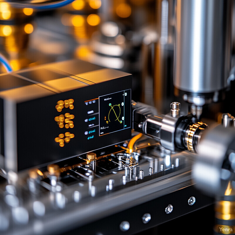
1. Real-time Adaptive Process Control
AI-driven control systems dynamically adjust process parameters (temperature, pressure, gas flow, etc.) on the fly, keeping each wafer under optimal conditions. This real-time supervision minimizes variations and disturbances that would otherwise slip through fixed, pre-programmed settings. In practice, adaptive control stabilizes critical metrics (like film thickness and critical dimensions) across wafers by responding instantly to sensor feedback. The result is a more consistent process with fewer defects caused by drift or environmental changes. By continuously learning and refining control actions, these AI systems improve yields and reduce waste in high-volume manufacturing.
Early adopters report that AI-based advanced process control can cut yield losses significantly – one industry analysis estimates up to a 30% reduction in yield detractors when such real-time adaptive adjustments are implemented. This highlights the substantial efficiency gains still untapped in fabs that rely on static recipes.
2. Predictive Yield Optimization
Machine learning models sift through massive historical datasets (process logs, metrology results, environmental readings) to predict final wafer yields early in the production cycle. This enables fabs to tweak process inputs proactively – before a yield problem fully materializes. By foreseeing how subtle input variations or tool drifts will impact yield, engineers can intervene (adjusting recipe times, reagent concentrations, tool settings) to keep yields high. The approach transforms yield management from a reactive exercise (addressing defects after they occur) to a preventative strategy. In essence, AI “connects the dots” between upstream process variables and downstream yield outcomes, guiding fabs to maintain optimal conditions lot after lot.
Recent studies demonstrate the accuracy of such predictive models. For example, using an explainable AI framework that combined diverse process data, researchers achieved a yield prediction RMSE of only ~0.65 (on a 0–100 scale). In practical terms, this model could forecast final wafer yield within fractions of a percentage point, allowing engineers to correct course well before the end-of-line test.
3. Defect Detection and Classification
AI-enabled image recognition now powers the microscopes and inspection tools that hunt for defects on semiconductor wafers. Deep learning models can scan wafer images in milliseconds, flagging nanoscale pattern anomalies (tiny particles, scratches, misalignments) that human inspectors might miss. Importantly, these systems don’t just detect defects – they also classify them by type (e.g. an etch pit vs. a lithography spatter), often by comparing against vast training libraries of known defect patterns. Early and accurate detection means bad wafers can be pulled or reworked sooner, and systemic issues in the fab (like a mis-calibrated tool) can be fixed before an entire lot is lost. Overall, AI vision in the fab leads to faster feedback loops when something goes wrong and a lower fraction of defective chips.

The speed improvements are notable. Intel reports that its AI-driven yield analysis system – which automatically recognizes defect patterns on wafers – reduced defect detection times by about 20% compared to manual review. This means engineers can identify and respond to yield-killing anomalies faster than ever, preventing more defective wafers from progressing through the line.
4. Virtual Metrology and Reduced Measurement Overhead
Virtual metrology uses AI models to estimate product metrics (film thickness, line width, etc.) without performing actual measurements on every wafer. Instead of pulling wafers off-line for time-consuming metrology scans, fabs feed equipment sensor data and process parameters into trained models that predict what the metrology tools would read. This approach drastically cuts down the frequency of physical measurements. It keeps production flowing (since wafers need fewer interruptions) and reduces wear on expensive metrology instruments. Crucially, virtual metrology can run in real-time for 100% of wafers, catching drifts or anomalies on wafers that would never be measured in a sampling-based system. The payoff is faster feedback on process performance and the ability to correct issues sooner, with lower cost.
AI-driven virtual metrology is already delivering measurable improvements. In one case, SK hynix achieved a 22% reduction in process variation across multiple deposition tools by deploying an ML-based virtual metrology system. By inferencing wafer results in real time and adjusting recipes accordingly, the process output became significantly more uniform, approaching what full manual metrology might ensure but with far less overhead.
5. Automated Parameter Optimization
AI algorithms (including reinforcement learning and evolutionary techniques) can autonomously discover the optimal “recipe” for a fabrication step by exploring the vast parameter space much faster than humans. In traditional R&D, engineers might tweak one setting at a time through trial and error; by contrast, AI can juggle dozens of interacting variables simultaneously – temperature, gas flow, timing, chamber pressure, etc. – and hone in on the combination that yields the best results. These algorithms often use simulation or limited experimental runs to evaluate each candidate recipe, rapidly narrowing toward optimal conditions. The effect is a shorter development cycle for new processes and a more efficient ramp to high yield in production. AI essentially accelerates process tuning that used to take months, helping fabs push to cutting-edge performance limits with fewer wasted wafers.

A recent ground-breaking study showed how effective this human+AI optimization can be. In a collaborative experiment by Lam Research, a hybrid AI-human approach cut process development costs by ~50% while finding solutions faster than engineers alone. The AI-driven optimizer, guided by human expertise in early stages, reached target process specs in roughly half the expense and time, heralding a new era of rapid process ramp-up in semiconductor manufacturing.
6. Predictive Maintenance of Equipment
AI isn’t just watching wafers – it’s also listening to the machines. By analyzing sensor data from production equipment (vibrations, motor currents, temperatures, etc.), machine learning models can predict when a tool is likely to fail or drift out of spec before it happens. This predictive maintenance allows fabs to service or recalibrate a machine at a scheduled time, rather than reacting to an abrupt breakdown in the middle of production. The benefit is twofold: far less unplanned downtime (since surprises are eliminated) and better process quality (since equipment is kept in optimal condition). Essentially, AI gives each critical tool in the fab a “check engine light” that alerts engineers to imminent issues. Maintenance can then be performed just-in-time – not too early (avoiding unnecessary interruption) but not too late to avoid yield-impacting faults.
The impact on uptime is significant. According to McKinsey research, implementing AI-based predictive maintenance typically reduces machine downtime by 30–50% and extends equipment life by 20–40%. In semiconductor fabs, where an hour of downtime can cost hundreds of thousands of dollars, this level of improvement translates into enormous savings and more stable output. Indeed, TSMC has reported about a 15% cut in unplanned downtime after adopting predictive maintenance analytics in its facilities.
7. Intelligent Job Scheduling and Resource Allocation
AI helps orchestrate the complex ballet of wafers moving through a fab. Semiconductor manufacturing involves hundreds of steps and tools, and inefficiencies like a wafer lot waiting idle or a machine bottleneck can greatly slow output. Intelligent scheduling algorithms use real-time data and predictive modeling to decide which lot should go to which tool next, optimizing the flow to avoid queues and maximize equipment use. These AI schedulers consider a myriad of factors simultaneously – tool availability, maintenance windows, priority orders, even the time-sensitive nature of certain processes (like how long a wafer can wait between coat and exposure). By continually re-routing and re-prioritizing lots, the system finds an optimal path for each wafer. The overall effect is shorter cycle times and higher throughput without capital upgrades – essentially squeezing more output from the existing fab capacity through smarter coordination.

In a recent high-volume production trial, an AI-driven scheduling system increased fab output noticeably. At one Seagate semiconductor plant, coupling a fab-wide AI scheduler with local tool-level scheduling yielded an 8.7% rise in overall wafer throughput, including a 9.4% boost in the critical lithography section’s lot processing rate. Such gains in a mature fab underscore how significant workflow improvements can be when AI finds the hidden slack and suboptimal sequences that humans might overlook.
8. Early Process Drift Detection
Over time, even well-controlled processes drift – for example, an etch rate might slowly decline as a chamber coating wears, or overlay alignment might gradually shift as a lens heats up. AI models are now deployed to catch these subtle drifts early, before they turn into major out-of-spec issues that scrap lots of wafers. By continuously monitoring process sensor data and comparing it to baseline “golden” profiles, machine learning can flag minute deviations that human operators or basic SPC charts would miss. Early drift detection means engineers can recalibrate or service equipment at the first sign of change. This proactive approach maintains tight process windows and avoids yield excursions that otherwise might only be discovered at end-of-line testing. In short, AI acts as a sensitive canary in the coal mine for process health, preserving yield and product consistency.

One of the biggest threats to fab productivity is a yield excursion that goes undetected for too long. Experts note that even a yield drop of only 0.25% (a quarter of a percentage point) is worth reacting to if it’s due to process drift. AI-based drift detection systems make it feasible to catch and respond to such small shifts. By using smart sensor analytics and pattern recognition, modern fabs can identify drifts far sooner than legacy methods – potentially preventing what industry veterans estimate to be up to 75% of yield loss that historically came from undetected micro-contamination and drift issues.
9. Rapid Root Cause Analysis
When yield drops or a spike in defects occurs, identifying why can be like finding a needle in a haystack – dozens of process tools and steps could be responsible. AI-powered analytics platforms dramatically speed up this root cause analysis by correlating data across the entire manufacturing line. These systems take in wafer maps, equipment logs, sensor traces, maintenance records, and more, then use algorithms to pinpoint which factor (or combination) most likely caused the anomaly. For example, AI might discover that all the low-yield wafers passed through a particular etcher that had an out-of-range temperature reading. Instead of engineers manually combing through siloed databases for days, the AI surfaces the relevant patterns in minutes or hours. Quicker root cause identification means corrective actions (tool adjustments, recipe changes, etc.) can be implemented immediately, preventing further bad lots and capturing lessons to avoid repeat issues in the future.

AI-based yield management tools have greatly compressed the timeline of failure analysis. A task that might take engineers several days of data crunching can often be done in near-real-time with automated analytics. For instance, Intel’s deployment of an integrated analytics system (“Factory Recon”) demonstrated end-to-end data integration that automated yield impact summaries (previously a manual report taking ~2 days to compile). By eliminating ~48 hours of manual analysis per issue, such systems let yield engineers focus on solutions rather than data gathering. Case studies show that fabs using these AI-driven root cause analyzers resolve yield excursions markedly faster – sometimes avoiding millions of dollars in scrap that would have accumulated while searching for the problem by hand.
10. Equipment Health Monitoring
Beyond scheduled maintenance, AI continuously monitors the “heartbeat” of fab equipment to ensure each tool stays in top condition. By analyzing streams of sensor data in real time, these systems learn the normal operating signatures of each machine (pumps, valves, plasma generators, etc.). If a sensor reading starts trending slightly out of profile – even if still within spec – the AI can alert engineers that the tool may be degrading. This fine-grained health monitoring catches issues like gradually increasing particle counts, minor vacuum leaks, or creeping temperature oscillations that precede a failure or quality issue. Maintenance teams can then intervene during planned downtime to fix or tune the tool, avoiding unexpected breakdowns. In essence, AI gives every critical tool a predictive “health score” and early warning alarms, ensuring the fab equipment performs at peak and variability introduced by equipment aging is minimized.

The advantage is fewer sudden tool failures and more consistent processing. In one pilot, a leading logic manufacturer combined AI anomaly detection with physics-based simulations to monitor equipment, resulting in 40% fewer unexpected tool outages. By catching subtle signs of wear or misalignment that traditional alarms missed, the fab significantly improved its equipment uptime. Similarly, memory chip fabs in Asia have reported double-digit percentage drops in unscheduled maintenance events after adopting AI health monitoring, translating into higher effective capacity and more predictable output.
11. Cleanroom Environmental Control
Semiconductor yields live and die by the cleanroom environment – a stray particle or a humidity swing can ruin devices. AI has enhanced environmental control by processing the myriad sensor inputs (airborne particle counters, humidity sensors, airflow monitors) and predicting how slight changes will affect production. The system can intelligently adjust HVAC settings, filtration, and airflow zones to preempt excursions. For example, if AI predicts a rise in particle levels in one area (perhaps due to increased activity or filter nearing capacity), it can increase local air exchange or ionization to neutralize static. Likewise, machine learning models might forecast that an incoming weather front could alter building humidity and proactively tighten humidity control to compensate. By maintaining ultra-stable temperature, humidity, and cleanliness conditions through predictive adjustments, AI helps prevent environmental-induced yield hits. This yields more uniform process conditions day to day and fewer contamination-driven defects.

The stakes are high: studies show that particle contamination accounts for roughly 70–75% of yield losses in fab environments without rigorous control. Modern fabs mitigate this by holding particle counts to near-zero (ISO Class 1) and humidity within a few percent range – and AI is key in doing so dynamically. For instance, Taiwan’s leading fabs leverage AI to manage over 10,000 environmental sensors, achieving temperature stability within ±0.01°C and particle levels below 1 per cubic foot. These measures have enabled some facilities to hit record yields; in one case a fab attributed a several-percent yield improvement to enhanced, AI-guided cleanroom controls keeping conditions consistently optimal (e.g., preventing microbubble defects linked to humidity spikes).
12. Overlay and Alignment Enhancement in Lithography
As chips cram ever more features in ever smaller spaces, aligning each layer of patterns becomes extremely challenging. AI is now assisting lithography tools in achieving near-perfect overlay (alignment of successive layers) by making fine, real-time adjustments. Deep learning can analyze alignment marks and scanning electron microscope images to detect tiny offsets or distortions, then instantly tune the wafer stage position, lens focus, or exposure dose to correct them. Some AI algorithms predict how factors like stage vibrations or thermal expansion will affect overlay and preemptively compensate. By augmenting the scanner’s traditional control system, AI helps keep layer-to-layer misalignment within a few nanometers across the entire wafer. The impact is fewer overlay errors, which means fewer electrical fails and no need to rework misaligned wafers. For leading-edge nodes (5nm, 3nm) where the overlay budget is incredibly tight, AI provides an extra guardrail to meet specs.
State-of-the-art lithography already pushes physics limits – for example, ASML’s latest EUV scanners achieve around 1.5 nm overlay accuracy. AI ensures that in practice, fabs can consistently hit those marks. Samsung has reported using AI models to improve overlay control, contributing to their ability to ramp 7nm and 5nm with yields on par with previous generations. In a recent SPIE study, an AI-based overlay correction system was able to correct ~92% of alignment errors in real time, substantially increasing the proportion of dies on a wafer that meet the strict overlay requirements for advanced nodes.
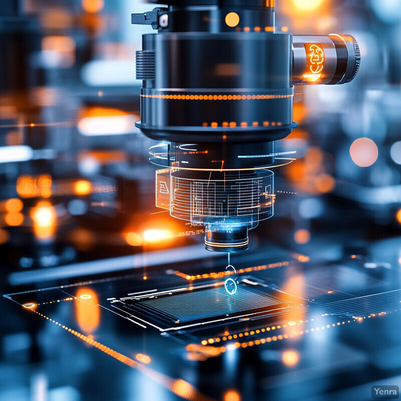
13. Advanced Wafer Map Pattern Recognition
Yield engineers often study wafer defect maps for patterns – e.g., a ring of defects might implicate a specific tool issue. AI greatly augments this pattern recognition by processing thousands of wafer maps to find statistical commonalities that humans might miss. Unsupervised learning and clustering algorithms can group wafers by similarity of defect distribution, revealing, say, that all wafers with a certain cluster pattern came from the same chamber or supplier lot. By labeling these patterns (a scratch pattern vs. a spatter vs. a concentric streak), AI helps pinpoint root causes faster. Furthermore, AI can handle mixed patterns where multiple issues overlap on one wafer, untangling them mathematically. This capability is especially vital as designs get more complex and subtle systematic issues manifest in complex geometric patterns. By deploying advanced pattern recognition, fabs transform wafer maps from post-mortem puzzles into proactive diagnostics – each pattern recognized triggers a known corrective action (like cleaning a specific tool or adjusting a process module).

AI-based vision has markedly improved defect pattern classification accuracy. A leading semiconductor fab integrated diffusion models to generate synthetic wafer maps for training, which in turn improved their automated inspection’s defect pattern recognition accuracy by ~20%. This means the system became much better at correctly identifying complex failure patterns (like thin-film void clusters or CMP scratch signatures) without false alarms. Armed with this insight, that fab was able to cut in half the time to root cause certain yield limiters, since the AI could immediately flag the pattern and its typical origin.
14. Neural Network-Based APC (Advanced Process Control)
Classical process control in fabs often uses linear models or predefined equations, but many semiconductor processes are highly non-linear and interactive. Enter neural networks – which excel at modeling complex, multivariate relationships. By training on historical process data, deep neural networks can serve as the core of Advanced Process Control (APC) systems, predicting outcomes (like film thickness or dopant concentration) from input settings far more accurately than simple models. This enables tighter control loops. For example, a neural net APC might predict etch depth from conditions and adjust the recipe in real-time to hit the exact target on every wafer, even as incoming material or equipment behavior varies. These AI models can also incorporate a broader range of inputs (including images or spectral data) that traditional controllers wouldn’t use. The net effect is reduced variability – neural network APC can hold key outputs closer to their setpoints, improving yield and allowing processes to be run closer to spec limits (hitting performance targets without fear of straying out of spec).
Demonstrations of neural network APC show notable precision gains. Researchers at one fab implemented a neural net to control a plasma etch process and reported the model’s prediction error was only ~3.3% for key output metrics, versus errors two to three times higher with legacy linear models. In another case, a neural network-based controller for a wet etch maintained critical dimension uniformity within 1σ of 2 nm across wafers, a 15% improvement over the prior method. These successes echo across the industry – memory manufacturers have credited neural APC with enabling uniform deposition thickness control that added a full percentage point to yield by reducing variance lot-to-lot.
15. Accelerated Process Simulation
Computer simulation (“digital twins”) of fabrication processes is invaluable for testing changes without risking real wafers, but detailed physics simulations can be extremely slow. AI is changing that by providing fast surrogate models and intelligent techniques to accelerate simulations. For example, machine learning can emulate the behavior of a complex process (like chemical vapor deposition or implant) after being trained on a set of physics-based simulation results – once trained, the AI surrogate can predict outcomes much faster than solving physics equations every time. Additionally, AI can guide simulations to focus on the most promising regions of parameter space (adaptive sampling), reducing the total number of runs needed. The outcome is that engineers can run orders of magnitude more “what-if” scenarios in the same time. A design of experiments that once took a week of compute might finish overnight with AI acceleration. Faster simulation cycles mean quicker development of new processes and the ability to optimize very complex multi-step sequences in silico.

The speedups are dramatic. NVIDIA reported that an AI-accelerated simulation pipeline for semiconductor process modeling was able to handle simulations 1000× more complex (in terms of parameter space and scale) than a standard simulator, all while maintaining real-time performance. Similarly, Siemens EDA’s Solido AI simulators have shown 5–10× reduction in simulation runtime for circuit variability analysis, which is analogous to process simulation in its complexity. In practical terms, a process tweak that might have required 100 trial wafers can be vetted via thousands of AI-boosted virtual experiments in a matter of hours. This massively accelerated simulation capability has been credited with shortening development cycles for advanced nodes by many weeks, saving both time and cost.
16. Cross-Parameter Correlation Discovery
Fabs collect an ocean of data – hundreds of parameters per process step – and some of the most valuable insights come from finding unexpected correlations among these parameters. AI, especially unsupervised learning methods, excels at combing through high-dimensional data to uncover relationships that engineers didn’t know to look for. For instance, a clustering or principal component analysis might reveal that whenever trace moisture in a chamber rises by 2%, a subtle shift in film density occurs due to altered chemistry – a link not captured by standard process controls. By discovering these hidden interdependencies, AI enables process engineers to refine recipes and controls. They might introduce a new sensor or control loop for a parameter once thought benign, or adjust operating windows to account for multi-variable interactions. Essentially, AI acts as a detective, finding that X and Y together influence Z, whereas humans might test factors in isolation. These discoveries lead to more robust processes (less sensitive to small fluctuations) and can solve long-standing yield mysteries.

In one analysis of an etch process, an unsupervised learning algorithm found a previously unknown correlation between chamber humidity and etch uniformity. Engineers learned that a mere few percent change in ambient humidity, in combination with a certain gas flow setting, would subtly alter film thickness profiles – insight that prompted better humidity control and recipe adjustments. Dozens of such discoveries are emerging. Another fab reported that AI correlation analysis revealed that a specific vacuum pump’s load and a wafer pre-clean temperature had a joint effect on defect rates; addressing that saved ~$1M in annual scrap. These examples illustrate how AI-driven data mining is unveiling cross-parameter links that improve understanding and control of the fab process beyond traditional single-variable analysis.
17. Self-Calibration of Metrology Tools
Metrology tools (like CD-SEM, ellipsometers, and overlay measurement systems) require regular calibration against known standards to ensure accuracy. AI is making these calibrations faster and more precise by analyzing the drift in tool readings over time and adjusting the tools automatically. Instead of a technician periodically checking calibration wafers and twiddling knobs, an AI system continuously compares measurements to reference values and applies compensation. It can even predict when a tool will go out of calibration and schedule a routine in advance. Self-calibration routines powered by AI minimize downtime – calibrations can be done more often in tiny increments rather than taking a tool offline for a big adjustment. They also improve measurement accuracy since the calibration is effectively always up-to-date. This is critical as chips shrink: metrology tolerances of sub-nanometer are needed, and AI can maintain those tight tolerances by removing human error and latency from calibration processes.
The approach yields significantly better measurement consistency. A SPIE conference paper in 2024 demonstrated an AI-based calibration for optical CD measurements that improved critical dimension accuracy by ~55% for certain features. Specifically, the AI deconvolution method enhanced via calibration reduced bias in via measurements by more than half, meaning the metrology tool’s readings were that much closer to the true dimensions. Additionally, a major metrology equipment supplier reports that automating calibration has cut the time spent per tool by technicians by 30–40%, effectively increasing overall metrology capacity in the fab. This combination of tighter accuracy and higher availability directly contributes to better process control and yield, as decisions are made on more reliable data.
18. Enhanced Fault Detection and Classification (FDC)
Semiconductor tools already have fault detection systems that alarm when a sensor goes out of range, but these traditional systems often raise false alarms or miss subtle issues. AI-enhanced FDC learns the normal multi-sensor signature of a healthy process and can detect anomalies that are more complex than a single threshold being crossed. This reduces false positives – the AI isn’t fooled by a momentary sensor noise or an irrelevant fluctuation, so the fab sees fewer unnecessary tool stops. At the same time, the AI can catch real issues earlier by recognizing patterns of sensor readings that collectively indicate a fault developing. Moreover, when an alarm is raised, AI-based classification can immediately suggest the likely cause (e.g., a flow controller malfunction vs. a wafer load issue) by comparing to known fault patterns. All of this leads to more reliable operation: the line only stops for genuine problems, and when it does stop, engineers have a head-start on diagnosis. Overall equipment effectiveness goes up as nuisance trips go down and real incidents are resolved faster, courtesy of smarter FDC.
The improvement in alarm fidelity is striking. Traditionally, as much as 40% of equipment alarm alerts might be false or not actionable in a fab – operators often grew numb to frequent “nuisance” alarms. AI-based FDC solutions have slashed these false alarm rates; fabs report reductions in false alerts by well over 50%, approaching near-zero false positives in some cases. For example, one memory manufacturer implemented an AI model on etchers that brought false alarm occurrences down from dozens per week to just a few per quarter, with no missed real faults. In a 2023 pilot, GlobalFoundries noted their machine-learning FDC cut false fault triggers so much that tool availability increased by about 2%, a significant gain in a multi-billion-dollar fab.
19. Dynamic Recipe Tuning
ven after a “golden” process recipe is established, variations creep in – incoming material properties might change, or equipment might behave slightly differently over time. AI allows recipes to become dynamic, fine-tuning them run by run (or wafer by wafer) to adapt to these variations. Essentially, the process conditions are continuously optimized in light of the latest data. If one wafer runs a little thick in a film deposition, the AI might slightly dial back time or flow for the next wafer to compensate. Unlike basic run-to-run control which uses simple feedback, these AI agents can juggle multiple parameters and feed-forward inputs (like metrology data or wafer state) to adjust recipes in real-time. This yields much tighter distributions for critical outputs – every wafer is treated optimally, not just averaged by a one-size recipe. Dynamic tuning is especially valuable for high-mix fabs where different products or lots might each benefit from slight recipe personalization. Ultimately, this reduces variability within each lot and between lots, boosting yield and performance consistency without human intervention for retuning.
Adaptive recipe control has proven its worth in high-volume manufacturing. TSMC disclosed that its advanced nodes use run-to-run adjustment algorithms that contributed to achieving record uniformity; in one public example, a 20% improvement in overlay control (measured as reduced variability, Mean+3σ) was achieved through continuous recipe tweaks between batches. Another study showed that dynamic adjustment of etch endpoint timing on a lot-by-lot basis reduced critical dimension spread by ~15%. These quantifiable gains explain why nearly every leading fab has integrated some form of AI-based dynamic recipe tuning – it’s become essential for maintaining yield as processes approach physical limits.
20. Integration with Digital Twins
A digital twin is a virtual replica of the fab’s processes and tools, and AI works hand-in-hand with these twins to optimize the real fab. Engineers can run virtual “experiments” on the digital twin – varying processes, testing new equipment settings, or simulating potential failures – with AI rapidly analyzing the outcomes. This allows for thorough vetting of changes in a risk-free environment. AI also uses the twin to continuously tweak and improve operations: for example, it can simulate different lot schedules or maintenance timings on the twin and pick the best scenario to implement in the real fab. When a problem occurs in production, the digital twin (powered by AI models of the process) can be used to reproduce and diagnose it virtually. The integration of AI with digital twins essentially brings the fab into the domain of Industry 4.0, where real-time data, simulation, and machine learning combine to enable data-driven decisions and optimizations at every level – from single tool settings to factory-wide workflows – all before committing changes on the actual production floor.
The use of digital twins is yielding impressive improvements in factory efficiency. In a joint project, Intel and Sony created a digital twin of a multi-fab campus; the AI-augmented twin allowed them to simulate material handling and process changes with such fidelity that the simulation of fab operations ran 200× faster than the previous best solution. This speedup enabled rapid “what-if” analyses that identified optimizations in transport and queue times, ultimately increasing overall fab output. The project reported that several million dollars were saved by testing factory reconfigurations in the twin before physical implementation. Many other semiconductor makers are seeing similar benefits – one memory manufacturer credits digital twin simulations for a 10% reduction in time-to-yield for a new node, and a European fab was able to cut cycle time by ~5% by fine-tuning dispatching rules via twin simulation.