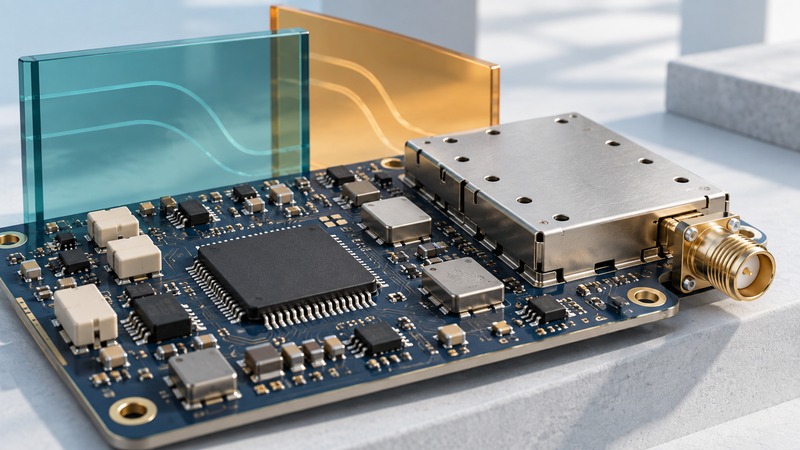
RF integrated circuits in a UHF RFID reader generate the interrogation signal and recover a much weaker tag response. Following those two paths explains why output power alone is a poor description of reader capability. The receiver must work while the reader is supplying RF energy to passive tags.
This is a guide to interpreting a block diagram and engineering discussion, not a build specification. Begin with the reader’s intended protocol, operating region and antenna arrangement. Keep those requirements separate from any example circuit’s historical component choices.
Trace the signal in each direction
On a small screen, scroll sideways to read all columns.
| Path or block | Purpose | Question for a design review |
|---|---|---|
| Transmit modulation and conversion | Form the interrogating waveform and place it at the RF carrier. | Which waveform, channel and timing requirements apply? |
| Power amplifier and output filtering | Deliver the intended signal level while controlling unwanted emissions. | At which reference plane is power specified? |
| Antenna sharing or separation | Connect transmit and receive paths to the antenna arrangement. | How much transmitter energy reaches the receiver? |
| Receive conversion and filtering | Recover the tag response in a band suitable for processing. | Which blockers, noise and bandwidth limit reception? |
| Gain, sampling and decoding | Present usable samples to the protocol processor. | Can the chain handle both weak responses and large residual signals? |
Analog Devices’ 2019 reader-front-end analysis illustrates forward-link power, reverse-link sensitivity and transmitter leakage in a specific vehicle-identification design. Its component choices and regulatory table describe that dated application; use its analysis method alongside current requirements for your own product.
Treat transmit leakage as a receive problem
In a shared-antenna reader, imperfect isolation and reflections allow part of the transmit signal into the receiver. This self-interference can limit useful sensitivity. The ADI analysis examines cancellation and conversion approaches; a design review should ask how residual leakage behaves across antenna mismatch, operating channels and gain settings.
Record sensitivity together with the waveform, data rate, error criterion and test configuration. A number measured with a quiet receiver input leaves simultaneous-transmit behavior unresolved. Ask for measurements that represent the complete reader and intended RF path, including any loss ahead of the receiver.
The older Design Note 381 on RFID receiver baseband circuits provides a focused example of filtering and gain after demodulation. It helps locate a fault by stage: an adequate RF signal can still be lost through inappropriate baseband bandwidth, gain or digitizer headroom.
Keep signal levels tied to a reference plane
The calculation is 30 − 40 = −10 dBm, then −10 − (−70) = 60 dB. The first result is an absolute power level; the second is a ratio in decibels. Before applying such arithmetic, place each measurement plane on the block diagram and include the losses between planes. Avoid mixing connector power, radiated power and chip-pin levels.
A large separation tells the engineer to investigate receiver headroom and interference handling. It does not directly specify an ADC bit count: filtering, cancellation, gain distribution, noise and bandwidth all affect what reaches the converter. Retain those assumptions in the review record.
Use the block diagram to ask better questions
- Where are transmit power and receive sensitivity measured, and what sits between those points and the antenna?
- Which operating channels, tag response modes and antenna conditions were tested?
- How are gain, filtering and leakage handling configured, and which settings are adaptive?
- What raw evidence supports a decoded response: waveform captures, packet/error counts and test conditions?
- Which power, thermal and supply conditions apply to the demonstrated result?
- What changes when the antenna, cable, enclosure, firmware or component revision changes?
For an intermittent fault, compare a known-good and failing configuration at the same defined interfaces using qualified RF test procedures. Preserve settings and captures before changing several variables. The object is to narrow the failing stage, then confirm the corrected system against its requirements.
Separate reader circuitry from tag-chip functions
A reader front end belongs to the powered interrogator. A passive tag’s chip, antenna and stored identity perform a different job. Use the tag-chip guide when the question concerns memory, encoding or tag selection.
At the end of a reader review, retain a marked block diagram, reference planes, configuration and evidence gaps. Revisit historical reference designs for explanation, and verify current component documentation and radio requirements before making an engineering or procurement decision.
Keep a working record
Download the editable working record (plain text). It includes purpose, instructions, evidence fields and this guide's source links. Save a separate copy for each evaluation and record unresolved issues with their owner.
Related reading
Researched and updated September 20, 2026. Recheck source documents when equipment, software or applicable requirements change.