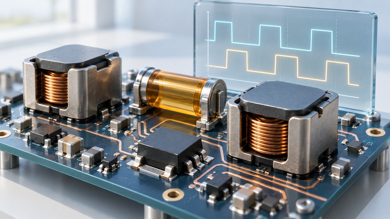
A SEPIC converter can produce a positive regulated DC output while its input moves above or below that output. Its useful flexibility comes with two inductive energy-storage paths, a coupling capacitor and switching stresses that must be checked across the input range.
This explanation assumes basic familiarity with voltage, current, inductors and switching regulators. It covers the conventional non-isolated, nonsynchronous topology at low DC voltage. An actual design requires the selected controller’s data sheet, component models, layout guidance and bench validation.
Follow the two switching states
In the basic circuit, the input feeds the first inductor. Its switching node connects to a switch to ground and to a coupling capacitor. The capacitor’s other side connects to the second inductor and the output diode; an output capacitor supplies the load between delivery intervals. The capacitor couples energy while blocking steady DC through that branch.
Texas Instruments’ June 2012 TPS55340 SEPIC application report, revision A includes the actual schematic and switching waveforms. Its component-selection procedure is specific to that controller and design.
On a narrow screen, scroll the table sideways. Keyboard users can focus the table region and use the arrow keys.
| State | Energy paths | Output behavior |
|---|---|---|
| Switch on | Inductor currents build; the coupling capacitor participates in energizing the second inductor. | The diode is reverse-biased and the output capacitor supplies the load. |
| Switch off | Both inductor paths contribute current through the forward-biased output diode; coupling-capacitor charge is replenished. | Energy reaches the load and output capacitor. |
Continuous-conduction mode (CCM) means the relevant inductor currents remain continuous through the switching cycle. At lighter loads a design may enter a different conduction mode, so use the appropriate controller model and equations.
Use the ideal relationship as a first check
For ideal steady-state CCM with negligible losses and ripple, Vout/Vin = D/(1 − D), where D is the fraction of each cycle for which the switch is on. Rearranging gives D = Vout/(Vin + Vout). Real diode drops, losses and controller limits alter the required duty ratio.
Fictional 10 V output example
For inputs of 5, 10 and 15 V, ideal duty ratios are respectively 10/15 = 0.667, 10/20 = 0.50 and 10/25 = 0.40. The ideal switch off-state voltage is approximately Vin + Vout: 15, 20 and 25 V.
These values explain the trend. Component voltage ratings also need appropriate margin for ripple, tolerances and transients. They are not a complete parts-selection specification.
Check current at the lowest input too. In a separate fictional operating point, 10 W output at an assumed 80% efficiency requires 12.5 W input. At 5 V that is 2.5 A average input current, before considering ripple and the switch current contributed by both inductor paths.
Evaluate the parts that carry the stress
TI’s March 2023 brief on SEPIC design describes its continuous input current, pulsed output current and control-loop tradeoffs. The conventional CCM power stage has a right-half-plane zero, which constrains practical control bandwidth. Use the controller’s compensation method and validate the response over operating conditions.
- Inductors: check peak current, saturation, winding loss and temperature rise. Coupled and separate inductors need the corresponding design model.
- Coupling capacitor: check voltage, ripple current, capacitance under bias and heating.
- Switch and diode: assess combined current paths, voltage stress and losses at input extremes.
- Output capacitor and layout: account for pulsed current, ripple and short high-current switching loops.
Compare a design against the actual operating envelope
Write down input minimum/maximum, output tolerance, load range, startup demand, temperature range and acceptable ripple. Include source impedance and sudden load changes. A battery or cable can produce conditions that an ideal bench supply hides.
Compare a SEPIC with other suitable buck-boost architectures using efficiency, thermal behavior, transient response, size and component stress at the same operating points. Then examine measured startup, load steps and temperatures on the actual board. If the input collapses or the converter reaches current limit at low input voltage, revisit the current budget and source capability.
The useful outcome is a justified topology choice and a validation plan. For broader loss and thermal accounting, see the power-converter guide.