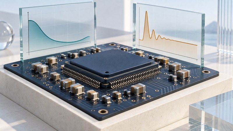
Power-integrity simulation asks whether a chip receives an acceptable supply voltage as its current demand changes. The relevant circuit includes the regulator, board conductors and capacitors, package interconnects, and the on-chip power and ground network within the chosen model boundary.
Start with the device's rail requirements, a current-demand model and the available board/package data. Define the observation point before judging a result: voltage at a regulator output and voltage at the die can differ. This guide concerns electronic power delivery; powertrain HIL simulation addresses a different testing task.
Choose the analysis for the question
On a narrow screen, scroll the table sideways. Keyboard users can focus the table region and use the arrow keys.
| Analysis | Question | Required inputs |
|---|---|---|
| DC resistance and IR drop | Does steady current leave enough voltage at the load? | Conductors, vias, package resistance, current distribution and temperature basis |
| Frequency-domain impedance | Which frequencies encounter a high-impedance delivery path? | Resistance, inductance, capacitance, ports and valid model bandwidth |
| Time-domain transient | Does a defined current change violate the rail limits? | Current waveform, regulator behavior, parasitics and initial conditions |
A resistive model supports a DC-drop calculation. Inductance, capacitance and regulator dynamics become consequential when the load changes quickly. Keep the power and return paths together so shared impedance and coupling are represented.
Altera's power-distribution-network resource distinguishes frequency-domain planning from device-specific time-domain requirements. Use the design method recommended for the exact device; a generic spreadsheet is a planning aid.
Allocate a voltage budget before optimizing
Fictional rail budget
A hypothetical 1.00 V rail has a 50 mV downward allowance at the chosen load point. Reserve 10 mV for regulator setting/tolerance and 15 mV for steady distribution drop. That leaves 25 mV for the defined transient excursion.
For a 5 A current step, a simple target-impedance screen is 25 mV ÷ 5 A = 5 milliohms. If the modeled DC path is 2 milliohms at 5 A, its steady drop is 10 mV, within the assumed 15 mV allocation.
These invented allocations illustrate the method. Check the actual device's upper and lower limits, tolerance definitions and load waveforms. The target-impedance screen still needs a stated frequency range and time-domain verification.
The Altera PDN tool user guide explains target impedance from allowed ripple and transient current. Preserve those definitions when transferring the method to a new rail; do not spend the entire tolerance budget independently on each source of error.
Interpret impedance peaks and decoupling
Real capacitors have series resistance and inductance, while their mounting and return paths add further parasitics. A nominal capacitance value therefore supplies incomplete information about high-frequency behavior. Model the selected components and connections over the required range.
Analog Devices' decoupling explanation describes local charge supply and capacitor impedance. Its high-speed ADC layout guidance connects supply behavior with the board's planes and physical layout.
When a frequency plot shows a peak, identify the contributing elements and check whether the load's current spectrum excites that region. Try a justified change in component choice or connection, then rerun the transient case. Adding capacitance indiscriminately can change resonances as well as stored charge.
Make the result traceable
Record the rail, port/reference location, current waveform, frequency range, model source and version, temperature assumptions and solver settings. Check that extracted models are used within their valid range and that the regulator representation matches the timescale being investigated.
- Check a simple DC case against Ohm's law and the expected current path.
- Verify model units, port ordering and return connections.
- Run representative load steps and inspect minimum voltage, overshoot and recovery.
- Compare with measurements using a documented probe location, bandwidth and measurement method.
- Archive failures and corrections with the exact configuration.
If simulation and measurement disagree, investigate the current stimulus, measurement location and omitted package or mounting parasitics before adjusting component values. A useful report ends with the tested rail conditions, remaining margin and limitations. It should let another engineer reproduce the result and see what remains unverified.
Power-integrity simulation review
Power-integrity simulation review — plain-text download. Save a copy and fill it in with your own information. The file includes instructions, assumptions and references so it can be used independently.