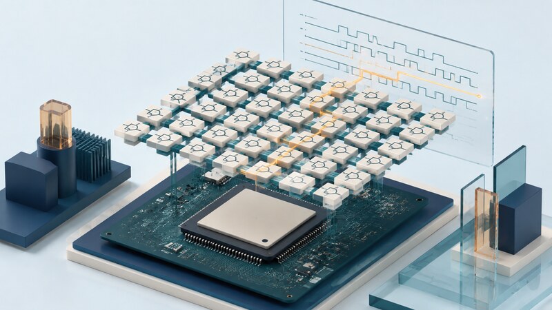
A field-programmable gate array (FPGA) contains configurable logic and interconnects that implement digital circuits. Designers describe registers, logic, and data paths, then use tools to map that design into the device.
An FPGA can perform many operations concurrently and support custom interfaces or pipelines. That flexibility comes with a hardware-design workflow. AI can draft HDL and testbenches, but compiling a design is only one step toward showing that it works.
Think in registers and concurrent logic
Hardware description languages such as Verilog, SystemVerilog, and VHDL express circuit structure and behavior. Synthesizable statements describe hardware that exists and operates over time. A loop may create repeated logic rather than execute like a loop on a processor.
Registers hold state at clock events; combinational logic computes outputs from its inputs. Width, signedness, reset behavior, and latency are part of the design. An extra pipeline stage can change when a result becomes valid even if the numerical answer is correct.
| Option | Reason to consider it | Cost to account for |
|---|---|---|
| Microcontroller | Software-driven control with standard peripherals. | Execution time and peripheral limits. |
| FPGA | Custom interfaces, parallel data paths, or precise digital sequencing. | HDL verification, timing closure, and board integration. |
| ASIC | A fixed design justified by production requirements. | Fabrication commitment and verification effort. |
Some FPGAs include processor cores, memory blocks, and specialized arithmetic resources. Evaluate the actual device and tool support rather than assuming every FPGA contains the same capabilities.
Worked example: a one-millisecond enable pulse
Specify reset priority and the phase of the first pulse. A testbench should check the interval between pulses, their single-cycle width, and restart behavior after reset. Keep downstream logic on the original clock and use the enable where appropriate, rather than treating an arbitrary logic output as a clock.
The one-millisecond period assumes the stated input frequency. Its absolute accuracy also depends on the clock source. This example is a logic specification, not a pin assignment or a complete board project.
Understand what each tool step establishes
Simulation tests modeled behavior against expected results. Synthesis turns supported HDL into a logic implementation. Placement and routing assign device resources and connections. Static timing analysis evaluates timing requirements against the implemented paths and supplied constraints.
AMD's FPGA verification overview describes simulation, timing analysis, and hardware debugging capabilities. These checks answer different questions; passing one does not replace the others.
Define the clocks and external timing requirements accurately. Review unconstrained paths and timing exceptions. A report can look clean because a path was excluded, not because the circuit meets its intended timing.
Check the boundaries of the design
Inputs arriving from another clock domain need a suitable clock-domain crossing design. A synchronizer appropriate for a single control bit does not automatically make a changing multi-bit bus coherent. Handshakes or asynchronous FIFOs may be needed for the transfer.
Mechanical buttons also bounce. Treat synchronization and debouncing as distinct tasks. Check I/O bank voltage, pin assignments, and board schematics before programming the device; HDL signal names do not establish electrical compatibility.
Test full and empty buffers, backpressure, simultaneous events, and reset during activity. Preserve the HDL, constraints, tool version, and build reports together so the implemented bitstream can be traced to its source.
Ask AI to challenge the specification
Review a proposed 50 MHz counter that generates a one-cycle enable every 50,000 cycles. Check widths, terminal count, reset priority, and pulse spacing. Write independent expected outcomes for simulation and identify assumptions that require timing or board-level verification.
A generated testbench can repeat the same mistaken assumption as the generated design. Compare both against an independently written requirement and small hand-worked cases. Inspect warnings about inferred latches, truncation, unused signals, and unsupported constructs.
Is an FPGA automatically better for AI?
No. Assess the model's operations, data movement, precision, latency, and development effort against other hardware. Parallel logic is useful when it addresses a measured requirement. A software prototype can establish that requirement before a custom pipeline is built.