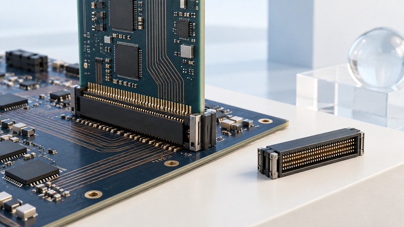
A high-speed board connector must fit the enclosure, survive assembly and service, and carry signals through the complete channel. Start with the mating geometry and electrical requirements together. A connector’s advertised data rate is a starting point for investigation; the PCB launches, routing, return paths and receiver determine the assembled result.
This guide focuses on backplanes and daughtercards. Prepare the board spacing and tolerances, signal list, power requirements, protocol and operating environment before comparing part numbers.
Define how the boards will meet
- Board orientation, slot pitch, mating direction, connector height and allowable misalignment.
- Guidance hardware, keying, retention, insertion force and access during servicing.
- Number of mating cycles and the environmental exposure of the assembly.
- Pin assignment, differential-pair organization, power contacts and ground/return contacts.
- PCB thickness, termination process, inspection access and supplier footprint requirements.
Check the tolerance stack across the enclosure, boards and connector locations. Nominal alignment in a drawing can conceal a difficult insertion at the tolerance extremes. Ask for the mating and unmating envelope, compatible counterpart and any required sequencing of ground, signal or power contacts. Verify hot-plug suitability explicitly if that is part of the product requirement.
A small footprint can also create difficult routing immediately beneath the connector. Review the proposed stack-up, via field and escape routing before committing to a board outline.
Ask for measurements with their boundaries
On a narrow screen, scroll the table horizontally. Keyboard users can focus the table region and use the arrow keys.
| Quantity | What it helps assess | Keep with the evidence |
|---|---|---|
| Insertion loss | Attenuation along the desired path versus frequency. | Reference planes, routing, de-embedding and mating configuration. |
| Return loss | Reflection from impedance discontinuities. | Port impedance, sign convention, frequency range and fixture treatment. |
| Crosstalk | Coupling from neighboring aggressor paths. | Near/far end, driven lanes, terminations and pair mapping. |
| Mode conversion | Transfer between differential and common-mode behavior. | Mixed-mode definition, port ordering and reference impedances. |
| Contact/power performance | Voltage drop, heating and service reliability. | Current distribution, ambient conditions, contact population and test duration. |
Samtec’s technical FAQ discusses high-speed characterization and how test assumptions affect results. Request the appropriate measurement or model for the actual mated part, not just another member of the family.
A Samtec connector characterization report is an example of the frequency- and time-domain evidence a supplier can provide. Read the report’s fixture and reference-plane description before comparing it with another vendor’s graph.
Use a channel budget as an early filter
Keep frequency and signaling mode explicit. A single loss number cannot describe a resonant notch, a reflection or coupling from an adjacent lane. Obtain suitable S-parameters, preserve the port map and verify that the model represents the proposed mounting and termination.
Review the launch before blaming the connector
The transition between PCB traces, vias and contacts can dominate an otherwise capable assembly. Samtec’s breakout-design discussion focuses on impairments in the board-attach region. Treat the recommended footprint and routing as engineering inputs that must be reconciled with your stack-up.
- Map the differential paths and return-current connections through the mating interface.
- Check via stubs, changes of routing layer and the available ground-via geometry.
- Model the proposed launch and surrounding aggressor lanes over the relevant bandwidth.
- Build a representative coupon or prototype with documented fixtures and access points.
- Compare measurement and model; resolve port mapping, fixture or assembly discrepancies before modifying the product design.
Use manufacturing feedback early. Press-fit or soldered termination, coplanarity, rework and inspection may determine whether an electrically promising option is practical to produce.
Release a reproducible interconnect definition
The release record should identify both mating parts, the footprint revision, stack-up, pinout, mechanical drawings and accepted test evidence. Preserve the model and its reference planes alongside measured results. State which operating corners were tested and which remain supported only by simulation.
If a link fails, compare the same pattern, transmitter setting, receiver configuration and measurement path across the suspect and reference assemblies. The ISI guide helps interpret channel-dependent behavior; the de-emphasis guide addresses transmitter compensation. Change one cause at a time so a successful retest explains something useful.
A purchasing substitution should repeat this evidence review. Similar contact count and outline do not establish the same mating behavior, footprint or high-speed channel.
Keep a working record
Download the high-speed board connectors worksheet (editable text). Save a copy for each comparison or test. It includes the example assumptions, fields for source references and space for your results.