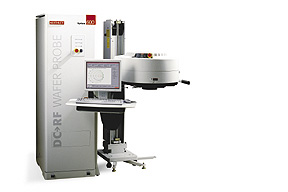
Keithley Instruments today announced availability of its S630DC/RF Parametric Testers with 40GHz RF measurement capabilities. These capabilities remove a major barrier to accurate characterization of ultra-thin gate dielectrics in advanced semiconductor devices.
Until now, an accurate method had not been identified for characterizing equivalent (electrical) thickness of certain gate dielectrics that were approaching the 0.5nm dimension, particularly in wireless communication devices. In testing these devices, inaccuracies can occur due to the high dissipation factor and phase error in the measurements, which may involve 3rd harmonic frequencies well above 20GHz. Keithley's high frequency (40GHz) RF measurement technique removes this barrier. This is accomplished by designing reliable RF connections into the test head and using per-pin electronics to achieve unequaled precision and repeatability. In addition, the system incorporates the leading vector network analyzer (VNA) and DC/RF probe card technology. When the system is used with a suitable test structure layout, it can execute independent DC and RF tests in parallel on separate probes, greatly reducing the time and cost of testing. The inherent DC resolution is 100aA and 100nV. This unique system also supports 300mm automation standards, and is compatible with both 200mm and 300mm probers.
Applications and Markets. Keithley's S600 Series represents one of the most versatile and widely accepted parametric test platforms available. These systems are used by semiconductor manufacturers around the world to assure product performance and reliability by measuring critical device parameters during product and process development, and in production. Ultra-thin gate dielectrics are a critical component of current processes. At the 100nm node of the International Technology Roadmap for Semiconductors (ITRS), gate dielectrics are reduced to a thickness of 1nm. Nodes beyond 100nm are slated for 0.6nm gate dielectric thickness by 2007. The 40GHz capability of the S630DC/RF test systems will allow accurate characterization of ultra-thin gate dielectrics well beyond the current design node. And because of the excellent 40GHz signal path, existing measurements of dielectric thickness made in the 3-6GHz range will have exceptional resolution that can reveal subtleties in dielectric structures that might not have been seen before. By supplying consistently accurate measurements, these systems cut down on rework and re-probes to verify readings--users get the right results the first time, and lower test costs.
Product Details. The S630DC/RF 40GHz test systems were developed in cooperation with leading semiconductor fabs and the industry's foremost suppliers of VNAs and DC/RF probe card systems. Anritsu Company's self-calibrating 40GHz VNA is an integral part of the measurement technique, along with GGB Industries' high frequency probe cards. Moreover, the test head design places complex impedance bias close to the DUT, which allows multi-bias capacitance measurements at the maximum frequency of the VNA. The high frequency reduces the dielectric's dissipation so that accurate measurements can be made. The DUT's interconnecting parasitic components are automatically de-embedded from the measurements. Standard quantum mechanical and poly depletion corrections can be applied to the extracted capacitance. The test head design also reduces stray capacitance and measurement settling time to maintain high throughput.
The S630DC/RF test systems come with a standard, well-supported test environment--the Keithley Test Environment (KTE). Test results can be easily imported into a variety of popular device modeling packages, such as BSIMPro(TM), IC-CAP, and UTMOST(TM). The KTE USERLIB macros calculate s-parameters and perform standard reductions of s-parameters to RF parameters, which can be used for characterization and process monitoring. The VNA, interconnects, probe card adapter, probe card, and calibration substrate are specified and calibrated as a complete system. Complete system calibration can be completed in approximately two minutes, giving device modeling engineers and production test engineers more time for reliable data collection and analysis.
KTE adapts easily and economically to new processes and applications. KTE and the S630DC/RF can characterize devices such as FRAMs, MRAMs, and PCRAM/OUMs. This parametric test system provides the high accuracy and precision needed by semiconductor fabs in measurements of complex impedances with high dissipation factors, which were not available with earlier AC measurement technologies. Moreover, this hardware and software forms a completely extendable characterization and modeling solution for current and future processes and materials.
For More Information. For more information on Keithley's Model S630DC/RF Parametric Testers, or any of Keithley's parametric test solutions, contact Keithley Instruments.
Keithley Instruments (now part of Tektronix) provides optical and electrical measurement solutions from DC to RF (radio frequency) to the wireless, semiconductor, optoelectronics, and other electronics manufacturing industries. Engineers and scientists around the world use Keithley's advanced hardware and software for process monitoring, production test, and basic research.