
Nanoimprint lithography (NIL) is a technique used in the field of nanotechnology for creating nanometer-scale patterns. This method is particularly important for fabricating structures and devices at the nanoscale. Here are the key points about NIL:
- Process: Nanoimprint lithography involves pressing a mold with the desired pattern into a substrate. The substrate is typically coated with a resist layer that deforms when the mold is pressed into it, transferring the pattern.
- High Resolution: NIL can create features smaller than 100 nanometers, making it suitable for extremely high-resolution patterning required in fields like electronics, photonics, and biotechnology.
- Cost-Effective: Compared to other lithography techniques, such as photolithography, NIL can be more cost-effective, especially for high-volume production.
- Applications: It's widely used in semiconductor manufacturing, for creating nanoscale devices, and in the development of advanced materials with unique properties at the nanoscale.
- Challenges: The technique faces challenges such as defect control, alignment accuracy, and the durability of the mold, especially when used for large-scale production.
Nanoimprint lithography represents a crucial advancement in nanotechnology, enabling the creation of complex nanostructures with high precision and efficiency.
 In 2007, HP began to reap returns from its ten-year investment in nanoscale electronics with the licensing of technology that could enable the fabrication of semiconductor chips significantly more powerful than those available today.
The technology involves a process called nanoimprint lithography (NIL) – a method of literally stamping out patterns of wires less than fifty atoms wide on a substrate. HP Labs researchers have created patented NIL technology, which has enabled the fabrication of laboratory prototype circuits with wire widths of fifteen nanometers.
Once the NIL master is created, copies can be stamped out quickly and inexpensively, like manufacturing CDs or phonograph records. The patterns are then filled in with metals.
HP has licensed the technology to Nanolithosolutions, which has developed a tool based on HP's technology. The tool consists of a module that fits into a mask aligne, used to create the patterns for wires and transistors on a substrate.
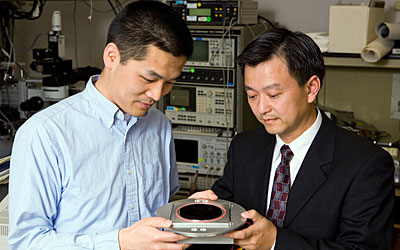
Pictured above: HP Labs researcher Wei Wu examines a device for creating future nanoscale computing chips with Bo Pi of Nanolithosystems.
"By building on HP's extensive research in nanoimprint lithography, we believe we have a tool that will enable reliable, repeatable processes for exploring biochips, photonics chips and many other applications," said Bo Pi.
Nanolithosolutions was created by Pi and Yong Chen, a UCLA professor and former member of HP Labs.
"Because HP and other companies need unique tools to conduct nanoscale research and development, we created the underlying technology that makes this tool possible," said Stan Williams, director of HP's Quantum Science Research. "But we rely on innovative companies like Nanolithosolutions to do the additional engineering necessary to make user-friendly tools commercially available. This will help create future generations of chips that will go beyond the capabilities of today's fabrication technologies."