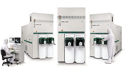
Applied Materials has unveiled a set of defect review and analysis tools for 65nm manufacturing. The new line of three systems sets the industry benchmark with 30nm sensitivity and throughputs of up to 1,800 defects per hour. Used in an optimized defect review strategy, these systems can accelerate customers' production ramp by rapidly identifying the root cause of systematic and yield-limiting defects.
The SEMVision G2 product line includes a new high productivity tool for performing routine defect review and production process monitoring. The new Applied SEMVision G2 Plus is the production workhorse system for volume defect review and material analysis, offering tilt and energy dispersive x-ray capabilities. As the ultimate system for inline root cause analysis, the recently introduced Applied SEMVision G2 focused ion beam system, with integrated focused ion beam technology, provides complete capability for embedded defect and electrical failure analysis.
"The Applied SEMVision G2 system has become an indispensable tool for root cause analysis in advanced fabs worldwide. Our new SEMVision G2 family is a direct response to customers' need for a set of next-generation tools optimized for different applications, enabling flexible system utilization during all stages of production ramp at the lowest overall cost," said Dr. Gilad Almogy of Applied Materials. "All three systems share the same proven platform, including the capability to share recipes, a common user interface and algorithms. This unique commonality shortens set-up time through extensive recipe sharing and provides high availability."
Applied's SEMVision technology, which features industry innovations such as multi-perspective imaging, materials analysis and inline focused ion beam, has rapidly expanded the use of scanning electron microscopes for defect analysis in manufacturing. The need for defect review has greatly increased and is now the third largest segment in the defect reduction market.
The new SEMVision family addresses the trend to achieve faster time to Resolution by harnessing the combined power of process and inspection expertise to dramatically cut the time and cost of resolving yield-limiting defects.
Applied Materials supplies equipment and services to the global semiconductor industry.